|
|
|
PDF 25P10AV Data sheet ( Hoja de datos )
| Número de pieza | 25P10AV | |
| Descripción | M25P10AV | |
| Fabricantes | ST Microelectronics | |
| Logotipo | ||
Hay una vista previa y un enlace de descarga de 25P10AV (archivo pdf) en la parte inferior de esta página. Total 51 Páginas | ||
|
No Preview Available !
M25P10-A
1 Mbit, serial Flash memory, 50 MHz SPI bus interface
Features
■ 1 Mbit of Flash memory
www.DataSheet4U■.comPage Program (up to 256 bytes) in 1.4 ms
(typical)
■ Sector Erase (256 Kbit) in 0.65 s (typical)
■ Bulk Erase (1 Mbit) in 1.7 s (typical)
■ 2.3 to 3.6 V single supply voltage
■ SPI bus compatible serial interface
■ 50 MHz Clock rate (maximum)
■ Deep Power-down mode 1 µA (typical)
■ Electronic signatures
– JEDEC standard two-byte signature
(2011h)
– RES instruction, one-byte signature (10h),
for backward compatibility
■ More than 20 years’ data retention
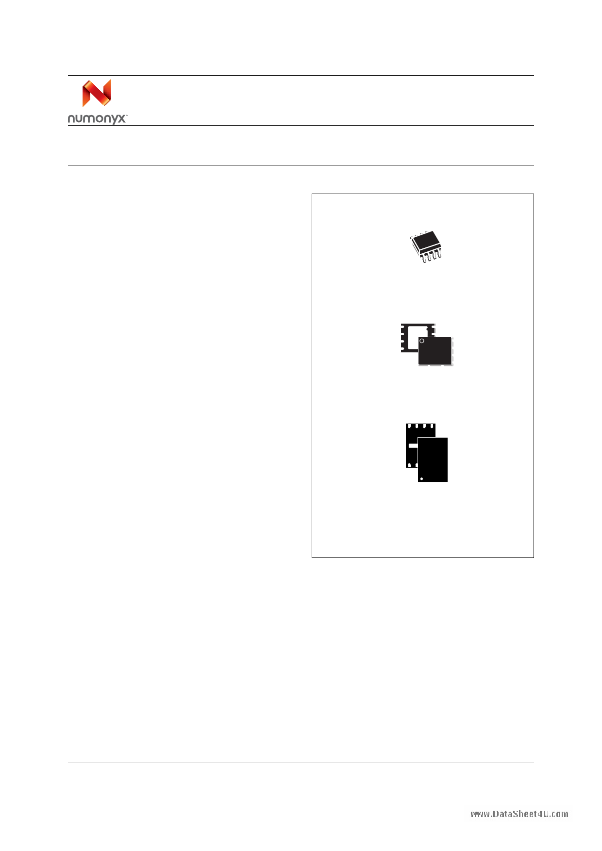
■ Packages
– ECOPACK® (RoHS compliant)
SO8 (MN)
150 mil width
VFQFPN8 (MP)
(MLP8)
UFDFPN8 (MB)
2 x 3 mm
December 2007
Rev 11
1/51
www.numonyx.com
1
1 page 
M25P10-A
List of figures
List of figures
Figure 1. Logic diagram . . . . . . . . . . . . . . . . . . . . . . . . . . . . . . . . . . . . . . . . . . . . . . . . . . . . . . . . . . . . 6
Figure 2. SO, VFQFPN and UFDFPN8 connections . . . . . . . . . . . . . . . . . . . . . . . . . . . . . . . . . . . . . . 7
Figure 3. Bus master and memory devices on the SPI bus . . . . . . . . . . . . . . . . . . . . . . . . . . . . . . . . . 9
Figure 4. SPI modes supported . . . . . . . . . . . . . . . . . . . . . . . . . . . . . . . . . . . . . . . . . . . . . . . . . . . . . 10
Figure 5. Hold condition activation . . . . . . . . . . . . . . . . . . . . . . . . . . . . . . . . . . . . . . . . . . . . . . . . . . . 14
Figure 6. Block diagram . . . . . . . . . . . . . . . . . . . . . . . . . . . . . . . . . . . . . . . . . . . . . . . . . . . . . . . . . . . 15
Figure 7. Write Enable (WREN) instruction sequence . . . . . . . . . . . . . . . . . . . . . . . . . . . . . . . . . . . . 17
www.DataSheet4UF.ciogmure 8. Write Disable (WRDI) instruction sequence . . . . . . . . . . . . . . . . . . . . . . . . . . . . . . . . . . . . 18
Figure 9. Read Identification (RDID) instruction sequence and data-out sequence . . . . . . . . . . . . . 19
Figure 10. Read Status Register (RDSR) instruction sequence and data-out sequence . . . . . . . . . . 21
Figure 11. Write Status Register (WRSR) instruction sequence . . . . . . . . . . . . . . . . . . . . . . . . . . . . . 23
Figure 12. Read Data Bytes (READ) instruction sequence and data-out sequence . . . . . . . . . . . . . . 24
Figure 13. Read Data Bytes at Higher Speed (FAST_READ) instruction sequence
and data-out sequence . . . . . . . . . . . . . . . . . . . . . . . . . . . . . . . . . . . . . . . . . . . . . . . . . . . . 25
Figure 14. Page Program (PP) instruction sequence . . . . . . . . . . . . . . . . . . . . . . . . . . . . . . . . . . . . . 27
Figure 15. Sector Erase (SE) instruction sequence . . . . . . . . . . . . . . . . . . . . . . . . . . . . . . . . . . . . . . . 28
Figure 16. Bulk Erase (BE) instruction sequence . . . . . . . . . . . . . . . . . . . . . . . . . . . . . . . . . . . . . . . . 29
Figure 17. Deep Power-down (DP) instruction sequence . . . . . . . . . . . . . . . . . . . . . . . . . . . . . . . . . . 30
Figure 18. Release from Deep Power-down and Read Electronic Signature (RES) instruction
sequence and data-out sequence . . . . . . . . . . . . . . . . . . . . . . . . . . . . . . . . . . . . . . . . . . . 32
Figure 19. Release from Deep Power-down (RES) instruction sequence . . . . . . . . . . . . . . . . . . . . . . 32
Figure 20. Power-up timing . . . . . . . . . . . . . . . . . . . . . . . . . . . . . . . . . . . . . . . . . . . . . . . . . . . . . . . . . 34
Figure 21. AC measurement I/O waveform . . . . . . . . . . . . . . . . . . . . . . . . . . . . . . . . . . . . . . . . . . . . . 36
Figure 22. Serial input timing . . . . . . . . . . . . . . . . . . . . . . . . . . . . . . . . . . . . . . . . . . . . . . . . . . . . . . . . 43
Figure 23. Write Protect Setup and Hold timing during WRSR when SRWD=1 . . . . . . . . . . . . . . . . . 43
Figure 24. Hold timing . . . . . . . . . . . . . . . . . . . . . . . . . . . . . . . . . . . . . . . . . . . . . . . . . . . . . . . . . . . . . 44
Figure 25. Output timing . . . . . . . . . . . . . . . . . . . . . . . . . . . . . . . . . . . . . . . . . . . . . . . . . . . . . . . . . . . 44
Figure 26. SO8 narrow – 8-lead plastic small outline, 150 mils body width, package outline . . . . . . . 45
Figure 27. VFQFPN8 (MLP8) 8-lead very thin fine pitch quad flat package no lead,
package outline. . . . . . . . . . . . . . . . . . . . . . . . . . . . . . . . . . . . . . . . . . . . . . . . . . . . . . . . . . 46
Figure 28. UFDFPN8 (MLP8) 8-lead ultra thin fine pitch dual flat package no lead,
2 x 3 mm package outline47
5/51
5 Page 
M25P10-A
4 Operating features
Operating features
4.1
www.DataSheet4U.com
Page Programming
To program one data byte, two instructions are required: Write Enable (WREN), which is one
byte, and a Page Program (PP) sequence, which consists of four bytes plus data. This is
followed by the internal Program cycle (of duration tPP).
To spread this overhead, the Page Program (PP) instruction allows up to 256 bytes to be
programmed at a time (changing bits from 1 to 0), provided that they lie in consecutive
addresses on the same page of memory.
For optimized timings, it is recommended to use the Page Program (PP) instruction to
program all consecutive targeted bytes in a single sequence versus using several Page
Program (PP) sequences with each containing only a few bytes (see Page Program (PP)
and Table 16: Instruction times (device grade 6)).
4.2 Sector Erase and Bulk Erase
The Page Program (PP) instruction allows bits to be reset from 1 to 0. Before this can be
applied, the bytes of memory need to have been erased to all 1s (FFh). This can be
achieved either a sector at a time, using the Sector Erase (SE) instruction, or throughout the
entire memory, using the Bulk Erase (BE) instruction. This starts an internal Erase cycle (of
duration tSE or tBE).
The Erase instruction must be preceded by a Write Enable (WREN) instruction.
4.3 Polling during a Write, Program or Erase cycle
A further improvement in the time to Write Status Register (WRSR), Program (PP) or Erase
(SE or BE) can be achieved by not waiting for the worst case delay (tW, tPP, tSE, or tBE). The
Write In Progress (WIP) bit is provided in the Status Register so that the application program
can monitor its value, polling it to establish when the previous Write cycle, Program cycle or
Erase cycle is complete.
4.4 Active Power, Standby Power and Deep Power-down modes
When Chip Select (S) is Low, the device is selected, and in the Active Power mode.
When Chip Select (S) is High, the device is deselected, but could remain in the Active Power
mode until all internal cycles have completed (Program, Erase, Write Status Register). The
device then goes in to the Standby Power mode. The device consumption drops to ICC1.
The Deep Power-down mode is entered when the specific instruction (the Deep Power-
down (DP) instruction) is executed. The device consumption drops further to ICC2. The
device remains in this mode until another specific instruction (the Release from Deep
Power-down and Read Electronic Signature (RES) instruction) is executed.
While in the Deep Power-down mode, the device ignores all write, program and erase
instructions (see Deep Power-down (DP)). This can be used as an extra software protection
mechanism, when the device is not in active use, to protect the device from inadvertent
write, program or erase instructions.
11/51
11 Page | ||
| Páginas | Total 51 Páginas | |
| PDF Descargar | [ Datasheet 25P10AV.PDF ] | |
Hoja de datos destacado
| Número de pieza | Descripción | Fabricantes |
| 25P10A | 1Mb 3V Serial Flash Embedded Memory | Micron |
| 25P10AV | M25P10AV | ST Microelectronics |
| Número de pieza | Descripción | Fabricantes |
| SLA6805M | High Voltage 3 phase Motor Driver IC. |
Sanken |
| SDC1742 | 12- and 14-Bit Hybrid Synchro / Resolver-to-Digital Converters. |
Analog Devices |
|
DataSheet.es es una pagina web que funciona como un repositorio de manuales o hoja de datos de muchos de los productos más populares, |
| DataSheet.es | 2020 | Privacy Policy | Contacto | Buscar |