|
|
PDF DP84902 Data sheet ( Hoja de datos )
| Número de pieza | DP84902 | |
| Descripción | 1.7 Encoder/Decoder Circuit | |
| Fabricantes | National Semiconductor | |
| Logotipo | ||
Hay una vista previa y un enlace de descarga de DP84902 (archivo pdf) en la parte inferior de esta página. Total 16 Páginas | ||
|
No Preview Available !
June 1994
DP84902
1 7 Encoder Decoder Circuit
General Description
The DP84902 is designed to perform the encoding and de-
coding for disk memory systems It is designed to interface
directly with Integrated Read Channel Products (such as
National Semiconductor’s DP84910) and with Disk Data
Controller Products with a 2-bit NRZ interface (such as Na-
tional Semiconductor’s Advanced Disk Controllers) This
Encoder Decoder (ENDEC) circuit employs a 2 3 (1 7) Run
Length Limited (RLL) code type and supports the hard sec-
tored format
The DP84902 has the option of selecting either TTL or ECL
compatible code output to interface with preamplifiers com-
monly used in high data rate applications This is accomm-
plished by the setting of a bit in the control register
The ENDEC also includes write data precompensation con-
trol circuitry which detects the need for write precompensa-
tion This circuitry issues early and late output signals nec-
essary for precompensation The precompensation informa-
tion is generated against a 2T pattern The precompensa-
tion circuitry can be bypassed by the setting of a bit in the
control register
A control reigster is included to configure the ENDEC and to
select device operation options such as output code inver-
sion differential code output bypassing of the encoder and
the use of an internal write clock
The DP84902 is available in 20-pin SO and 20-pin SSO
packages
Features
Y Operates at 2-bit Non-Return to Zero (NRZ) Data Rates
up to 50 Mbits second
Y Single a5V Power Supply Operation
Y Low Power Dissipation when TTL compatible code out-
put is selected 150 mW at 50 Mbits second NRZ Rate
Y TTL Compatible Inputs and Outputs
Y ECL Compatible Code Outputs (patented) are control
register selectable
Y Two-bit NRZ Interface
Y Supports Write Data Precompensation with Early and
Late output signals
Y Selectable use of either an Internal or External Write
Clock
Y Power Down Mode Included
Y DC-Erasure is available to support Analog Flaw Map-
ping Testing
Y Bypass Mode available which permits Un-Encoded Test
Patterns to be issued at the CODEOUT Pin
Block Diagram
FIGURE 1 DP84902 ENDEC Block Diagram
TL F 11963 – 1
TRI-STATE is a registered trademark of National Semiconductor Corporation
IBM is a registered trademark of International Business Machines Corporation
C1995 National Semiconductor Corporation TL F 11963
RRD-B30M105 Printed in U S A
1 page 
Control Register Operating Conditions are guaranteed over operating conditions (see table) unless
otherwise specified
Symbol
Parameter
Typ
Min Max Units
(Note 1)
Test
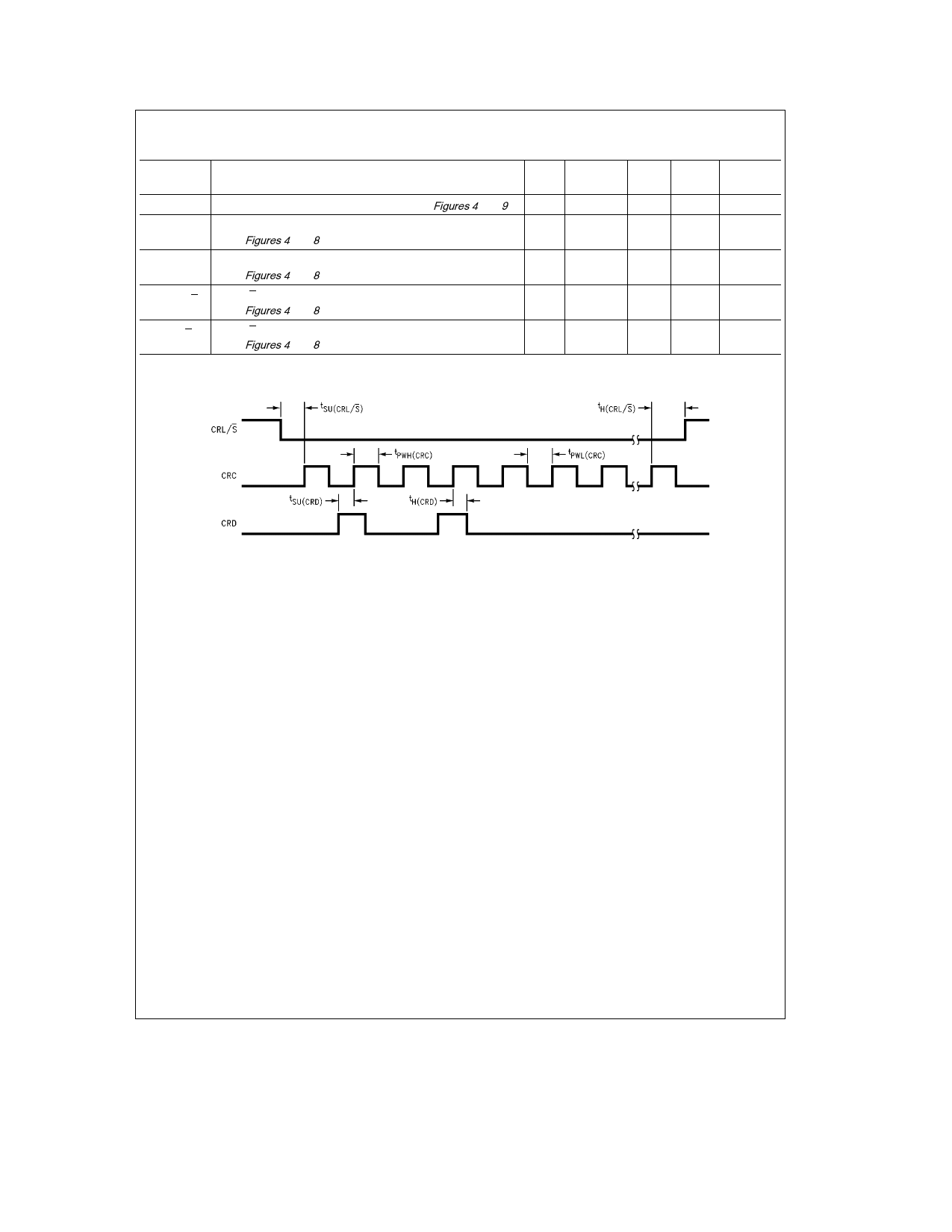
tPW(CRC)
tSU(CRD)
CRC Pulse Width (positive or negative) (see Figures 4 and 9 )
CRD Setup Time with respect to CRC (positive edge)
(see Figures 4 and 8 )
14
5
ns (Note A)
ns (Note A)
tH(CRD)
CRD Hold Time with respect to CRC (positive edge)
(see Figures 4 and 8 )
5
ns (Note A)
tSU(CRL S)
CRL S Setup Time with respect to CRC (positive edge)
(see Figures 4 and 8 )
5
ns (Note A)
tH(CRL S)
CRL S Hold Time with respect to CRC (positive edge)
(see Figures 4 and 8 )
5
ns (Note A)
Note 1 Typical values are specified at 25 C and 5V supply
Note A This parameter is guaranteed by outgoing testing
FIGURE 4 Control Register Timing Diagram
TL F 11963 – 4
5
5 Page 
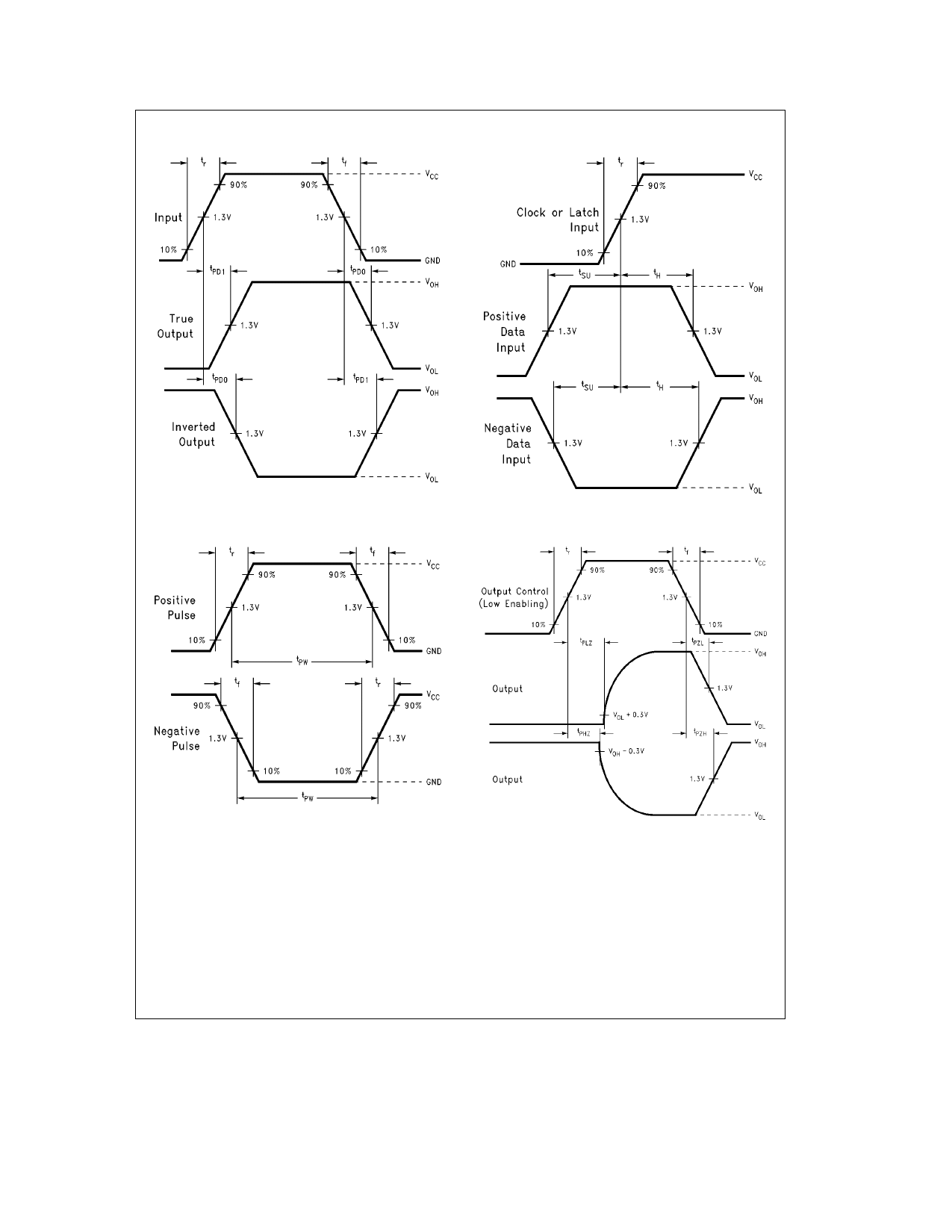
AC Electrical Characteristics Waveforms
TL F 11963 – 11
FIGURE 7 Propagation Delay Waveforms
TL F 11963 – 12
FIGURE 8 Setup and Hold Time Waveforms
TL F 11963 – 13
FIGURE 9 Input or Output Pulse Width Waveforms
TL F 11963 – 14
FIGURE 10 TRI-STATE Output Enable and Disable
Waveforms
11
11 Page | ||
| Páginas | Total 16 Páginas | |
| PDF Descargar | [ Datasheet DP84902.PDF ] | |
Hoja de datos destacado
| Número de pieza | Descripción | Fabricantes |
| DP8490 | Enhanced Asynchronous SCSI Interface | National Semiconductor |
| DP84902 | 1.7 Encoder/Decoder Circuit | National Semiconductor |
| DP84902 | DP84902 17 Encoder/Decoder Circuit (Rev. A) | Texas Instruments |
| Número de pieza | Descripción | Fabricantes |
| SLA6805M | High Voltage 3 phase Motor Driver IC. |
Sanken |
| SDC1742 | 12- and 14-Bit Hybrid Synchro / Resolver-to-Digital Converters. |
Analog Devices |
|
DataSheet.es es una pagina web que funciona como un repositorio de manuales o hoja de datos de muchos de los productos más populares, |
| DataSheet.es | 2020 | Privacy Policy | Contacto | Buscar |
