|
|
|
PDF AN10E40 Data sheet ( Hoja de datos )
| Número de pieza | AN10E40 | |
| Descripción | Field Programmable Analog Array | |
| Fabricantes | Anadigm | |
| Logotipo | ||
Hay una vista previa y un enlace de descarga de AN10E40 (archivo pdf) en la parte inferior de esta página. Total 37 Páginas | ||
|
No Preview Available !
AN10E40
Field Programmable Analog Array
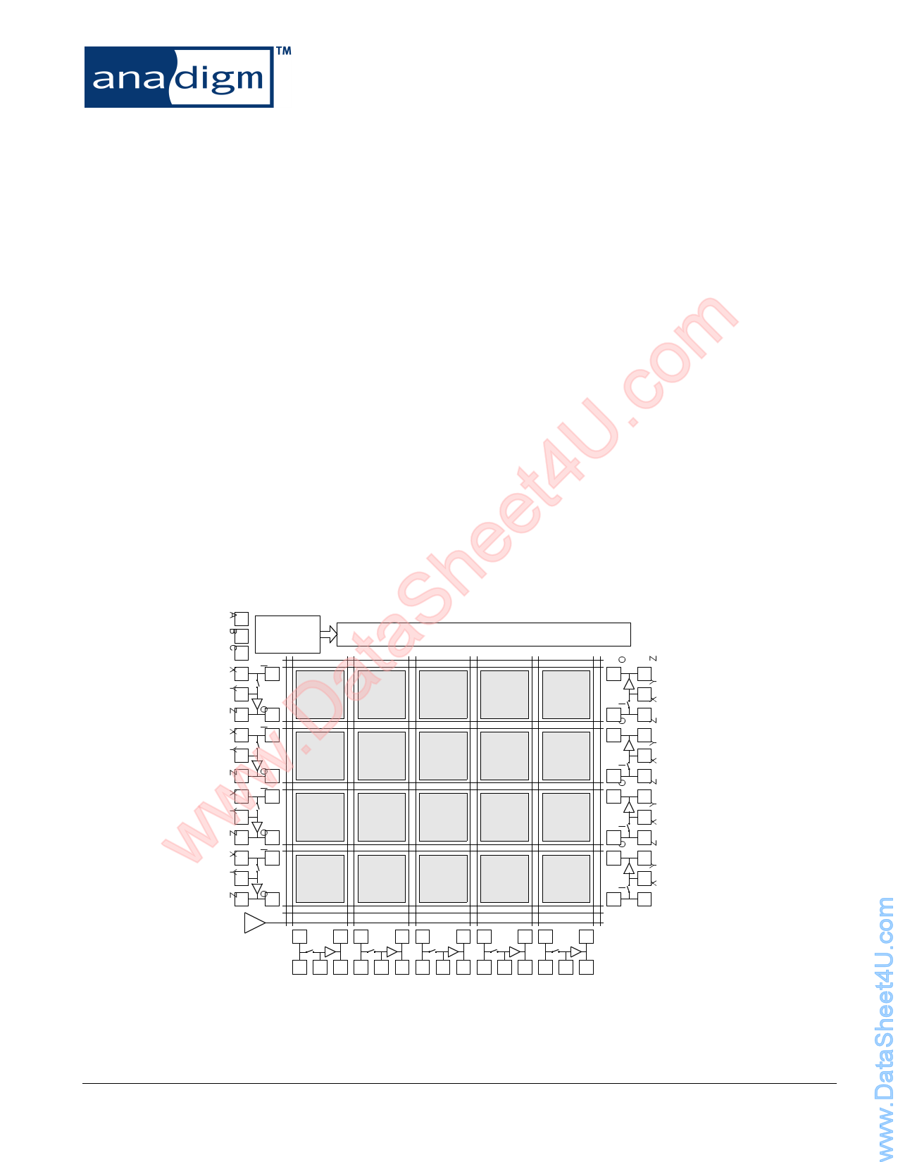
The AN10E40 brings to analog what FPGAs brought to digital; extremely rapid production and prototype circuit
realization with field re-programmability. The AN10E40 consists of a 4 x 5 matrix of fully configurable switched
capacitor cells, enmeshed in a fabric of programmable interconnect resources. These programmable features are
directed by an on-chip SRAM configuration memory. The SRAM configuration memory is initialized on power up
via an off chip serial PROM or through the AN10E40Õs standard microprocessor peripheral interface.
A configuration memory image is easily constructed using the companion AnadigmDesigner¨ software which
includes an extensive library of adjustable, proven, pre-built functions. The configurable analog blocks are often
consumed one at a time, though some of the more complex library functions may consume two or more blocks.
Specialized IO cells surround the core to bring your analog signals in and out of the array.
The AN10E40 coupled with the intuitive AnadigmDesigner¨ software gives both digital and analog designers a
mcompetitive advantage in designing analog circuits that canÕt really be compared to any other design system in
existence. Quickly constructed, accurate, drift free, temperature compensated and programmable analog circuits
oare now yours. Imagine the power of programmable with the versatility of analog.
.cBenefits
U• Extremely Rapid Analog Design Ð Minutes not weeks to re-spin a new design idea
t4• In Circuit Programmable Ð Behavior can be changed as fast as 125 microseconds
• Re-Configurable Using Conventional Logic, Serial PROMs or Microcontrollers
e• Extremely Stable over Voltage and Temperature
• Flexible Internal Clock and Routing Resources
• No Component Aging
• No More Trimming Components
e• Reliable and Repeatable Performance
• No More Tuning Components
ShConfig. Logic
Configuration Data Shift Register
taCAB
CAB
CAB
CAB
CAB
.DaCAB
CAB
CAB
CAB
CAB
www CAB
CAB
CAB
CAB
CAB
CAB
CAB
CAB
CAB
CAB
Vref
I OI OI OI OI O
XY Z XY Z XY Z XYZ XY Z
Anadigm¨
UM020800-U005
1 page 
AN10E40 Data Manual 1
Features of AN10E40
• 20 Programmable Analog Cells
• 13 Analog IO Cells
• 2 Spare Op-Amps
• 8 Bit Programmable Internal Vref Source
• 4 Programmable Internal Clock Sources
• Easy Power-On-Reset Self Boot Using Serial PROM
• Microprocessor Boot Option
• Intuitive Design Software
• Drift Free Designs
• Rapidly Configurable
Available IPmodule Functions
• Gain Stages
• Summing Amplifiers
• Sample and Hold
• Track and Hold
• High, Low and Band Pass/Stop Filters
• High Q, Low Q Filters
• Cosine Filters
• Full and Half Non/Inverting Rectifiers
• Non/Inverting Comparators
• 1 and 2 Input Comparators
• DC Reference Voltage Sources
• Limiters
• Schmitt Triggers
• Non/Inverting Integrators
• Differentiators
• New IP Modules Continuously Available
How It Works
On power up, the AN10E40Õs reset circuitry initializes the configuration engine. The configuration engine takes over
and first examines the state of the Mode port. The pin settings of the Mode port determine which of the boot
methods should be exercised. One popular option is to boot from an off chip Serial PROM. The configuration
engine takes care of taking data out of the Serial PROM and loading it into on-chip configuration SRAM. The whole
boot process takes just a few milliseconds. Once the configuration SRAM has been loaded, the analog circuitry is
automatically enabled and the configuration engine idled. The chip now performs the analog functions according to
the configuration bit stream just loaded.
Creating a configuration bit stream is no more complicated than using the device itself. The AnadigmDesigner¨
design tool provides the user an intuitive drag and drop GUI in which you simply select several of the IPmodule
functions from the extensive library, drop them onto a graphical representation of the chip, fill in some parametric
information about the IPmodule, wire up the internal and I/O connections, and hit a button to generate the bit
stream (or download it directly to the device on your bench).
The device internals are more complicated than the easy to use device may lead you to believe. The AN10E40
array is based on programmable switched capacitor op-amp cells with very flexible internal and external connection
and clocking resources. The AnadigmDesigner¨ and the associated IPmodule library shields the user from these
complexities.
Switched capacitor circuits are remarkably stable over voltage, temperature and device aging. Using the AN10E40
for your analog circuit realization allows you to rest assured knowing that once a circuit has been designed, it will
continue perform as expected. Say goodbye to trim pots.
Another advantage of this technology is the tremendous decrease in design time. Along with the elimination of trim
pots, youÕll also be able to clear your bench of all the normal discrete R and C components. ÒPrototypingÓ is now a
drag and drop computer exercise. A simple push of a button and your design is downloaded into the AN10E40
nearly instantaneously.
The kicker to all of this is that it is infinitely re-programmable. If a single set of analog functions is not sufficient for
your system, then you can load new configuration files into the AN10E40 with only a very small interruption to the
analog signal stream. Consider how filter parameters can be changed to adapt to varying input signal conditions.
Consider how a single physical circuit can be used in all of your different system designs. Consider all the
advantages that programmable analog will bring to your designs.
Anadigm¨
UM020800-U005
5 Page 
2nd Order Sallen-Key Filter for Output Smoothing
AN10E40 Data Manual 7
IO
XYZ
20
dB
0
-20
2nd Order
-40dB/Decade
-40
-60
Frequency [Hz]
Figure 6. A 2nd Order Sallen-Key Filter for Output Smoothing
4th Order Sallen-Key Filter for Output Smoothing
I OI O
XYZXYZ
20
dB
0
-20
-40
-60
4th Order
-80dB/Decade
Frequency [Hz]
Figure 7. A 4th Order Sallen-Key Filter for Output Smoothing
Here, the first stage of filtering is handled by an otherwise unused IO cell. It can instead be one of the two spare op-
amps the AN10E40 provides. (See the Pin Out Description section for a description of pins 24, 25, 74 and 75.)
2nd Order Sallen-Key Filter for Input Anti-Aliasing
Anadigm¨
IO
XYZ
20
dB
0
-20
-40
-60
2nd Order
-40dB/Decade
Frequency [Hz]
Figure 8. A 2nd Order Sallen-Key Filter for Input Anti-Aliasing
UM020800-U005
11 Page | ||
| Páginas | Total 37 Páginas | |
| PDF Descargar | [ Datasheet AN10E40.PDF ] | |
Hoja de datos destacado
| Número de pieza | Descripción | Fabricantes |
| AN10E40 | Field Programmable Analog Array | Anadigm |
| Número de pieza | Descripción | Fabricantes |
| SLA6805M | High Voltage 3 phase Motor Driver IC. |
Sanken |
| SDC1742 | 12- and 14-Bit Hybrid Synchro / Resolver-to-Digital Converters. |
Analog Devices |
|
DataSheet.es es una pagina web que funciona como un repositorio de manuales o hoja de datos de muchos de los productos más populares, |
| DataSheet.es | 2020 | Privacy Policy | Contacto | Buscar |