|
|
PDF N74F604D Data sheet ( Hoja de datos )
| Número de pieza | N74F604D | |
| Descripción | Dual octal latch 3-State | |
| Fabricantes | Philips | |
| Logotipo |  |
|
Hay una vista previa y un enlace de descarga de N74F604D (archivo pdf) en la parte inferior de esta página. Total 7 Páginas | ||
|
No Preview Available !
Philips Semiconductors
Dual octal latch (3-State)
Product specification
74F604
FEATURES
• High impedance NPN base inputs for reduced loading
(20µA in High and Low states)
• Stores 16-bit–wide Data inputs, multiplexed 8-bit outputs
• 3-State outputs
• Power supply current 75mA typical
DESCRIPTION
The 74F604 multiplexed latch is ideal for storing data from two input
buses, A or B, and providing data from either the A or B latches to
the output bus. Organized as 8-bit A and B latches, the latch outputs
are connected by pairs to eight 2-input multiplexers. A Select
(SELECT A/B) input determines whether the A or B latch contents
are multiplexed to the eight 3-State outputs. Data entered from the B
inputs are selected when SELECT A/B is Low; data from the A
inputs are selected when SELECT A/B is High. Data enters the
latches when the Latch Enable (LE) input is Low and is latched on
the LE rising edge. The outputs are enabled when LE is High and
disabled when LE is Low.
PIN CONFIGURATION
LE 1
SELECT A/B 2
A0 3
B0 4
A1 5
B1 6
A2 7
B2 8
A3 9
B3 10
Q3 11
Q2 12
Q1 13
GND 14
28 VCC
27 A4
26 B4
25 A5
24 B5
23 A6
22 B6
21 A7
20 B7
19 Q7
18 Q6
17 Q5
16 Q4
15 Q0
SF01115
TYPE
74F604
TYPICAL
PROPAGATION
DELAY
7.5ns
TYPICAL SUPPLY CURRENT
(TOTAL)
75mA
ORDERING INFORMATION
DESCRIPTION
28-pin plastic DIP
COMMERCIAL RANGE
VCC = 5V ±10%, Tamb = 0°C to +70°C
N74F604N
28-pin plastic SOL
N74F604D
INPUT AND OUTPUT LOADING AND FAN-OUT TABLE
PINS
DESCRIPTION
A0–A7, B0–B7 Data inputs
SELECT A/B Select input
LE Latch Enable input (active Low)
Q0–Q7
Data outputs
NOTE:
One (1.0) FAST unit load is defined as: 20µA in the High state and 0.6mA in the Low state.
74F (U.L.)
HIGH/LOW
1.0/0.033
1.0/0.033
1.0/0.033
150/40
LOAD VALUE
HIGH/LOW
20µA/20µA
20µA/20µA
20µA/20µA
3mA/24mA
1990 Mar 01
1 853–0029 98991
1 page 
Philips Semiconductors
Dual octal latch (3-State)
Product specification
74F604
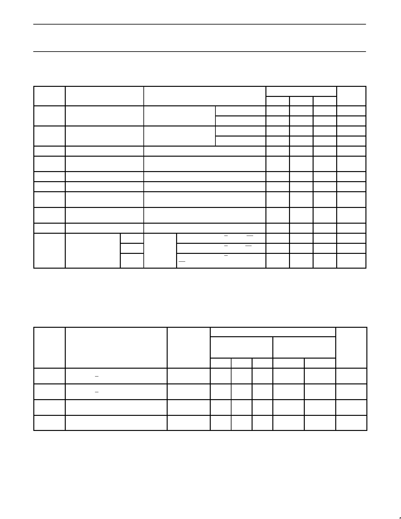
DC ELECTRICAL CHARACTERISTICS
(Over recommended operating free-air temperature range unless otherwise noted.)
SYMBOL
PARAMETER
TEST CONDITIONS1
LIMITS
MIN TYP2 MAX
UNIT
VOH High-level output voltage
VCC = MIN, VIL = MAX,
VIH = MIN, IOH = MAX
VOL Low-level output voltage
VCC = MIN, VIL = MAX,
VIH = MIN, IOL = MAX
VIK Input clamp voltage
VCC = MIN, II = IIK
II
Input current at maximum input
voltage
VCC = 0.0V, VI = 7.0V
±10%VCC
±5%VCC
±10%VCC
±5%VCC
2.4
2.7 3.4
0.35 0.50
0.35 0.50
–0.73 –1.2
100
V
V
V
V
V
µA
IIH
IIL
IOZH
High-level input current
Low-level input current
Off state output current,
High-level voltage applied
VCC = MAX, VI = 2.7V
VCC = MAX, VI = 0.5V
VCC = MAX, VO = 2.7V
20 µA
–20 µA
50 µA
IOZL
Off state output current,
Low-level voltage applied
VCC = MAX, VO = 0.5V
–50 µA
IOS
Short-circuit output current3
VCC = MAX
–60
–150
mA
ICCH
An, Bn, SELECT A/B = 4.5V, LE = ↑
60 82
mA
ICC Supply current (total) ICCL VCC = MAX An, Bn, SELECT A/B=GND, LE = ↑
ICCZ
An, Bn, SELECT A/B = GND,
LE = GND
75 100
75 100
mA
mA
NOTES:
1. For conditions shown as MIN or MAX, use the appropriate value specified under recommended operating conditions for the applicable type.
2. All typical values are at VCC = 5V, Tamb = 25°C.
3. Not more than one output should be shorted at a time. For testing IOS, the use of high-speed test apparatus and/or sample-and-hold
techniques are preferable in order to minimize internal heating and more accurately reflect operational values. Otherwise, prolonged shorting
of a High output may raise the chip temperature well above normal and thereby cause invalid readings in other parameter tests. In any
sequence of parameter tests, IOS tests should be performed last.
AC ELECTRICAL CHARACTERISTICS
SYMBOL
PARAMETER
tPLH
tPHL
tPLH
tPHL
tPZH
tPZL
tPHZ
tPLZ
Propagation delay
SELECT A/B to Qn (B latch)
Propagation delay
SELECT A/B to Qn (A latch)
Output Enable time
to High or Low level
Output Disable time
from High or Low level
TEST
CONDITION
Waveform 1
Waveform 2
Waveform 4
Waveform 5
Waveform 4
Waveform 5
LIMITS
VCC = +5V
Tamb = +25°C
CL = 50pF, RL = 500Ω
MIN TYP MAX
VCC = +5V ± 10%
Tamb = 0°C to +70°C
CL = 50pF, RL = 500Ω
MIN MAX
5.0 7.0 9.0
6.0 8.5 10.5
4.5
5.5
10.0
11.5
6.0 8.0 10.0
4.0 6.5 8.5
5.5
3.5
11.5
9.0
5.0 7.5 9.5
5.0 7.5 9.5
4.5
4.5
10.5
11.0
5.0 7.0 9.5
5.0 7.0 9.5
4.5
4.5
11.0
11.0
UNIT
ns
ns
ns
ns
1990 Mar 01
5
5 Page | ||
| Páginas | Total 7 Páginas | |
| PDF Descargar | [ Datasheet N74F604D.PDF ] | |
Hoja de datos destacado
| Número de pieza | Descripción | Fabricantes |
| N74F604D | Dual octal latch 3-State | Philips |
| N74F604N | Dual octal latch 3-State | Philips |
| Número de pieza | Descripción | Fabricantes |
| SLA6805M | High Voltage 3 phase Motor Driver IC. |
Sanken |
| SDC1742 | 12- and 14-Bit Hybrid Synchro / Resolver-to-Digital Converters. |
Analog Devices |
|
DataSheet.es es una pagina web que funciona como un repositorio de manuales o hoja de datos de muchos de los productos más populares, |
| DataSheet.es | 2020 | Privacy Policy | Contacto | Buscar |
