|
|
|
PDF 93C56 Data sheet ( Hoja de datos )
| Número de pieza | 93C56 | |
| Descripción | 3-Wire Serial EEPROMs | |
| Fabricantes | ATMEL Corporation | |
| Logotipo | ||
Hay una vista previa y un enlace de descarga de 93C56 (archivo pdf) en la parte inferior de esta página. Total 21 Páginas | ||
|
No Preview Available !
Features
• Low-voltage and Standard-voltage Operation
– 2.7 (VCC = 2.7V to 5.5V)
– 1.8 (VCC = 1.8V to 5.5V)
• User-selectable Internal Organization
– 1K: 128 x 8 or 64 x 16
– 2K: 256 x 8 or 128 x 16
– 4K: 512 x 8 or 256 x 16
• Three-wire Serial Interface
• 2 MHz Clock Rate (5V)
• Self-timed Write Cycle (10 ms max)
• High Reliability
– Endurance: 1 Million Write Cycles
– Data Retention: 100 Years
• Automotive Grade, Extended Temperature and Lead-Free/Halogen-Free
Devices Available
• 8-lead PDIP, 8-lead JEDEC SOIC, 8-lead EIAJ SOIC, 8-lead MAP, 8-lead TSSOP,
and 8-ball dBGA2 Packages
Description
The AT93C46/56/66 provides 1024/2048/4096 bits of serial electrically erasable pro-
grammable read-only memory (EEPROM), organized as 64/128/256 words of 16 bits
each (when the ORG pin is connected to VCC), and 128/256/512 words of 8 bits each
(when the ORG pin is tied to ground). The device is optimized for use in many indus-
trial and commercial applications where low-power and low-voltage operations are
essential. The AT93C46/56/66 is available in space-saving 8-lead PDIP, 8-lead
JEDEC SOIC, 8-lead EIAJ SOIC, 8-lead MAP, 8-lead TSSOP, and 8-lead dBGA2
packages.
The AT93C46/56/66 is enabled through the Chip Select pin (CS) and accessed via a
three-wire serial interface consisting of Data Input (DI), Data Output (DO), and Shift
Clock (SK). Upon receiving a Read instruction at DI, the address is decoded and the
data is clocked out serially on the DO pin. The Write cycle is completely self-timed,
and no separate Erase cycle is required before Write. The Write cycle is only enabled
when the part is in the Erase/Write Enable state. When CS is brought high following
the initiation of a Write cycle, the DO pin outputs the Ready/Busy status of the part.
The AT93C46/56/66 is available in 2.7V to 5.5V and 1.8V to 5.5V versions.
Table 1. Pin Configurations
Pin Name
Function
CS Chip Select
SK Serial Data Clock
DI Serial Data Input
DO Serial Data Output
GND
Ground
VCC
Power Supply
ORG
Internal Organization
DC Don’t Connect
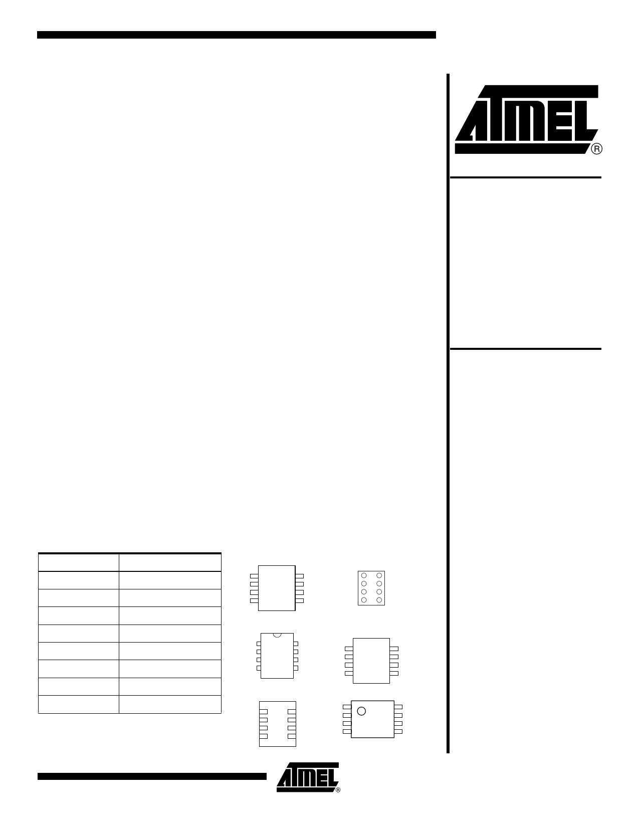
8-lead SOIC
8-lead dBGA2
CS 1
SK 2
DI 3
DO 4
8 VCC
7 DC
6 ORG
5 GND
VCC
DC
ORG
GND
8
7
6
5
1 CS
2 SK
3 D1
4 D0
8-lead PDIP
CS 1
SK 2
DI 3
DO 4
8 VCC
7 DC
6 ORG
5 GND
8-lead SOIC
Rotated (R)
(1K JEDEC Only)
DC
VCC
CS
SK
1
2
3
4
8 ORG
7 GND
6 DO
5 DI
8-lead MAP
VCC 8
DC 7
ORG 6
GND 5
1 CS
2 SK
3 DI
4 DO
8-lead TSSOP
CS 1
SK 2
DI 3
DO 4
8 VCC
7 DC
6 ORG
5 GND
Three-wire
Serial
EEPROMs
1K (128 x 8 or 64 x 16)
2K (256 x 8 or 128 x 16)
4K (512 x 8 or 256 x 16)
AT93C46
AT93C56(1)
AT93C66(2)
Note: 1. This device is not recom-
mended for new designs.
Please refer to AT93C56A.
2. This device is not recom-
mended for new designs.
Please refer to AT93C66A.
0172Z–SEEPR–9/05
1
1 page 
AT93C46/56/66
Table 5. Instruction Set for the AT93C46
Instruction SB
Op
Code
Address
x 8 x 16
READ
1 10
A6 – A0
A5 – A0
EWEN
ERASE
WRITE
ERAL
1 00 11XXXXX 11XXXX
1 11
1 01
A6 – A0
A6 – A0
A5 – A0
A5 – A0
1 00 10XXXXX 10XXXX
Data
x 8 x 16
D7 – D0
D15 – D0
WRAL
1 00 01XXXXX 01XXXX D7 – D0 D15 – D0
EWDS
1 00 00XXXXX 00XXXX
Note: The Xs in the address field represent DON’T CARE values and must be clocked.
Comments
Reads data stored in memory, at
specified address
Write enable must precede all
programming modes
Erases memory location An – A0
Writes memory location An – A0
Erases all memory locations. Valid
only at VCC = 4.5V to 5.5V
Writes all memory locations. Valid
only at VCC = 4.5V to 5.5V
Disables all programming instructions
Table 6. Instruction Set for the AT93C56(1) and AT93C66(2)
Op
Instruction SB Code
Address
x 8 x 16
READ
1 10
A8 – A0
A7 – A0
Data
x 8 x 16
EWEN
ERASE
WRITE
ERAL
1 00 11XXXXXXX 11XXXXXX
1 11
1 01
A8 – A0
A8 – A0
A7 – A0
A7 – A0
D7 – D0
D15 – D0
1 00 10XXXXXXX 10XXXXXX
WRAL
1 00 01XXXXXXX 01XXXXXX D7 – D0 D15 – D0
EWDS
1 00 00XXXXXXX 00XXXXXX
Notes: 1. This device is not recommended for new designs. Please refer to AT93C56A.
2. This device is not recommended for new designs. Please refer to AT93C66A.
Comments
Reads data stored in memory, at
specified address
Write enable must precede all
programming modes
Erases memory location An – A0
Writes memory location An– A0
Erases all memory locations. Valid
only at VCC = 4.5V to 5.5V
Writes all memory locations. Valid
only at VCC = 5.0V ±10% and Disable
Register cleared
Disables all programming instructions
0172Z–SEEPR–9/05
5
5 Page 
AT93C46/56/66
AT93C46 Ordering Information(1)
Ordering Code
Package
Operation Range
AT93C46-10PI-2.7
AT93C46-10SI-2.7
AT93C46R-10SI-2.7
AT93C46W-10SI-2.7
AT93C46-10TI-2.7
8P3
8S1
Industrial
8S1
(−40°C to 85°C)
8S2
8A2
AT93C46-10PI-1.8
AT93C46-10SI-1.8
AT93C46R-10SI-1.8
AT93C46W-10SI-1.8
AT93C46-10TI-1.8
8P3
8S1
Industrial
8S1
(−40°C to 85°C)
8S2
8A2
AT93C46-10PU-2.7
AT93C46-10PU-1.8
AT93C46-10SU-2.7
AT93C46-10SU-1.8
AT93C46W-10SU-2.7
AT93C46W-10SU-1.8
AT93C46-10TU-2.7
AT93C46-10TU-1.8
AT93C46Y1-10YU-2.7
AT93C46Y1-10YU-1.8
AT93C46Y5-10YU-2.7
AT93C46Y5-10YU-1.8
AT93C46U3-10UU-2.7
AT93C46U3-10UU-1.8
AT93C46-W2.7-11(2)
AT93C46-W1.8-11(2)
8P3
8P3
8S1
8S1
8S2
8S2
8A2
8A2
8Y1
8Y1
8Y5
8Y5
8U3-1
8U3-1
Die Sale
Die Sale
Lead-free/Halogen-free/
Industrial Temperature
(−40°C to 85°C)
Industrial
(−40°C to 85°C)
Notes: 1. For 2.7V devices used in the 4.5V to 5.5V range, please refer to performance values in the Table 3 on page 3 and Table 4 on
page 4.
2. Available in waffle pack and wafer form, order as SL719 for wafer form. Bumped die available upon request.
8P3
8S1
8S2
8A2
8U3-1
8Y1
8Y5
−2.7
−1.8
R
Package Type
8-lead, 0.300" Wide, Plastic Dual Inline Package (PDIP)
8-lead, 0.150" Wide, Plastic Gull Wing Small Outline (JEDEC SOIC)
8-lead, 0.200" Wide, Plastic Gull Wing Small Outline (EIAJ SOIC)
8-lead, 0.170" Wide, Thin Shrink Small Outline Package (TSSOP)
8-ball, Die Ball Grid Array Package (dBGA2)
8-lead, 4.90 mm x 3.00 mm Body, Dual Footprint, Non-leaded, Miniature Array Package (MAP)
8-lead, 2.00 mm x 3.00 mm Body, Dual Footprint, Non-leaded, Miniature Array Package (MAP)
Options
Low Voltage (2.7V to 5.5V)
Low Voltage (1.8V to 5.5V)
Rotated Pinout
0172Z–SEEPR–9/05
11
11 Page | ||
| Páginas | Total 21 Páginas | |
| PDF Descargar | [ Datasheet 93C56.PDF ] | |
Hoja de datos destacado
| Número de pieza | Descripción | Fabricantes |
| 93C56 | 3-Wire Serial EEPROMs | ATMEL Corporation |
| 93C56 | 16Kbit/ 8Kbit/ 4Kbit/ 2Kbit/ 1Kbit and 256bit 8-bit or 16-bit wide | STMicroelectronics |
| 93C56 | Electrically Erasable Programmable Memories | National Semiconductor |
| 93C56 | 2K 5.0V Automotive Temperature Microwire Serial EEPROM | Microchip Technology |
| Número de pieza | Descripción | Fabricantes |
| SLA6805M | High Voltage 3 phase Motor Driver IC. |
Sanken |
| SDC1742 | 12- and 14-Bit Hybrid Synchro / Resolver-to-Digital Converters. |
Analog Devices |
|
DataSheet.es es una pagina web que funciona como un repositorio de manuales o hoja de datos de muchos de los productos más populares, |
| DataSheet.es | 2020 | Privacy Policy | Contacto | Buscar |