|
|
|
PDF MAX202 Data sheet ( Hoja de datos )
| Número de pieza | MAX202 | |
| Descripción | +5V-Powered / Multichannel RS-232 Drivers/Receivers | |
| Fabricantes | Maxim Integrated | |
| Logotipo | ||
1. MAX202 Hay una vista previa y un enlace de descarga de MAX202 (archivo pdf) en la parte inferior de esta página. Total 23 Páginas | ||
|
No Preview Available !
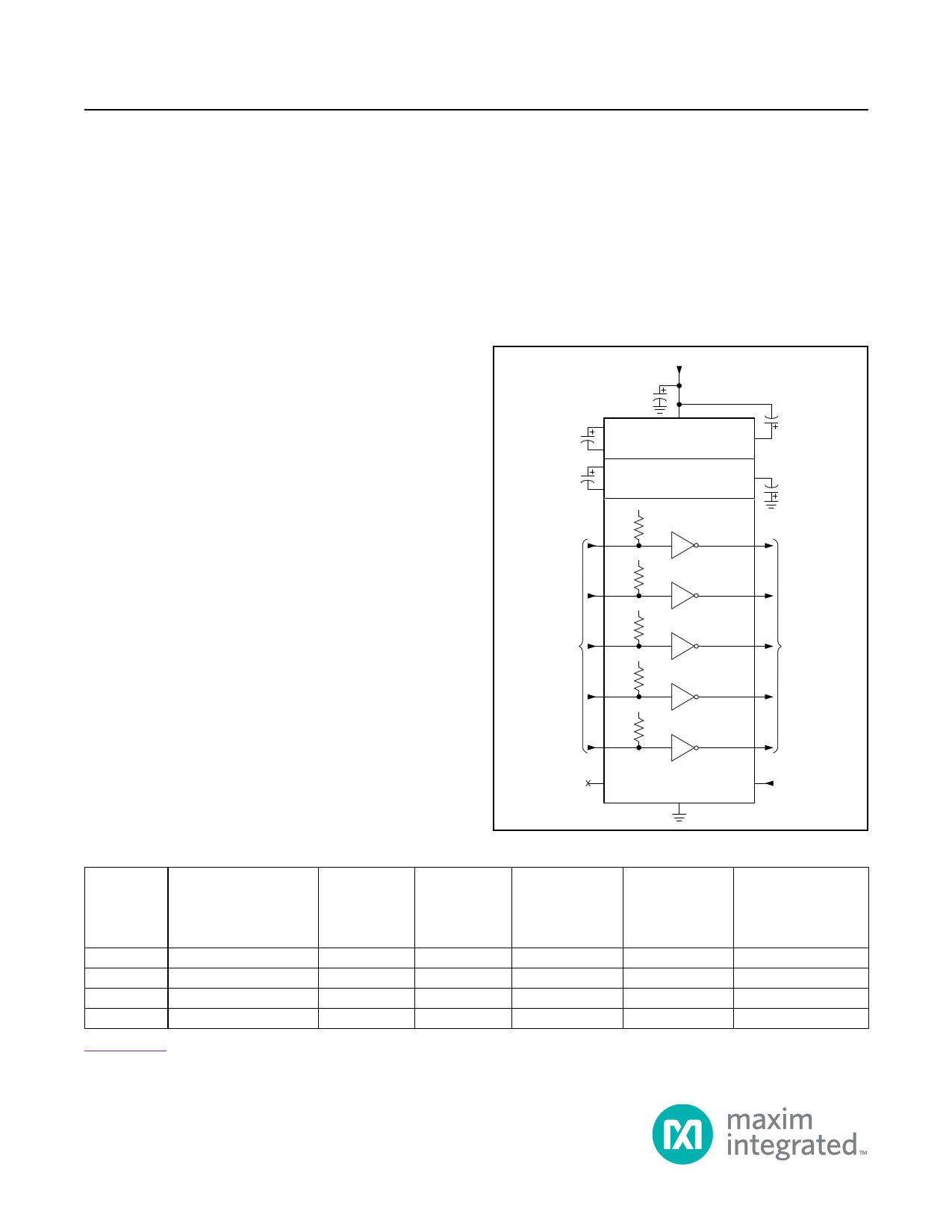
MAX200–MAX209/
MAX211/MAX213
+5V, RS-232 Transceivers
with 0.1μF External Capacitors
General Description
MAX200-MAX209, MAX211, and MAX213 are a family
of RS-232 and V.28 transceivers with integrated charge
pump circuitry for single +5V supply operation.
The drivers maintain the ±5V EIA/TIA-232E output signal
levels at data rates in excess of 120kbps when loaded in
accordance with the EIA/TIA-232E specification.
The MAX211 and MAX213 are available in a 28-pin, wide
small-outline (SO) package and a 28-pin shrink small-
outline (SSOP) package, which occupies only 40% of the
area of the SO. The MAX207 is available in a 24-pin SO
package and a 24-pin SSOP. The MAX203 and MAX205
use no external components and are recommended for
applications with limited circuit board space.
Benefits and Features
●● Saves Board Space
• Integrated Charge Pump Circuitry
Eliminates the Need for a Bipolar ±12V Supply
Enables Single Supply Operation From Either +5V
or 9V to +12V
• Integrated 0.1μF Capacitors (MAX203, MAX205)
• 24 pin SSOP Package Saves Up to 40% Versus
SO Package
●● Saves Power for Longer Battery Operation
• 5μW Shutdown Mode (MAX200, MAX205,
MAX206, MAX211)
• 75μW Ring Indicator Monitoring with Two Active
Receivers (MAX213)
Applications
●● Battery-Powered Equipment
●● Handheld Equipment
●● Portable Diagnostics Equipment
Typical Operating Circuit
+5V INPUT
0.1µF
+6.3V
0.1µF
+16V
8 C1+
10 C1-
11
C2+
12
C2-
0.1µF
7
VCC
+5V TO +10V
VOLTAGE DOUBLER
+10V TO -10V
VOLTAGE INVERTER
+5V
5 T1IN
400kΩ
T1
+5V
4 T2IN
400kΩ
T2
+5V
TTL/CMOS
INPUTS
14 T3IN
400kΩ
T3
+5V
15 T4IN
400kΩ
T4
+5V
19 T5IN
400kΩ
T5
V+ 9
0.1µF
+6.3V
13
V-
0.1µF
+16V
T1OUT 2
T2OUT 3
T3OUT 1
RS-232
OUTPUTS
T4OUT 20
T5OUT 16
N.C. 18
MAX200
GND
6
17 SHDN
Selector Guide
PART
POWER-SUPPLY
VOLTAGE (V)
NUMBER
OF RS-232
DRIVERS
MAX200
MAX201
MAX202
MAX203
+5
+5 and +9.0 to +13.2
+5
+5
Selector Guide continued at end of data sheet.
5
2
2
2
NUMBER
OF RS-232
RECEIVERS
0
2
2
2
NUMBER OF
RECEIVERS
ACTIVE IN
SHUTDOWN
0
0
0
0
NUMBER OF
EXTERNAL
CAPACITORS
(0.1μF)
4
2
4
None
LOW-POWER
SHUTDOWN/TTL
THREE-STATE
Yes/No
No/No
No/No
No/No
19-0065; Rev 8; 1/15
1 page 
MAX200–MAX209/
MAX211/MAX213
+5V, RS-232 Transceivers
with 0.1μF External Capacitors
+5.5V
0.1µF
0.1µF
0.1µF
+5.5V
0V OR +5.5V
DRIVE
+5.5V (0)
ISHDN
0.1µF
C1+ VCC
C1- MAX200
C2+
MAX205
MAX206
MAX211
C2- +5.5V MAX213
400kΩ
TIN
T1 T0 T5
V+
V-
TOUT
ROUT
R1 T0 R5
EN (EN)
SHDN
(SHDN)
GND
RIN
5kΩ
0.1µF
3kΩ
+5.5V
NOTE 1: ( ) ARE FOR MAX213.
NOTE 2: CAPACITORS CAN BE POLARIZED OR UNPOLARIZED.
Figure 1. Shutdown Current Test Circuit
EN
INPUT +3V
0V
OUTPUT ENABLE TIME
RECEIVER
OUTPUT
CL = 150pF
+3.5V
+0.8V
+3V
EN 0V
INPUT
OUTPUT ENABLE TIME
RECEIVER
OUTPUTS
VOH
VOL
VOH - 0.1V
+ 2.5V
RL = 1kΩ
VOL + 0.1V
NOTE: POLARITY OF EN IS REVERSED FOR THE MAX213.
Figure 2. Receiver Output Enable and Disable Timing
Detailed Description
The MAX200–MAX209/MAX211/MAX213 consist of three
sections: charge-pump voltage converters, drivers (trans-
mitters), and receivers. Each section is described in detail.
+5V to ±10V Dual Charge-Pump
Voltage Converter
The +5V to ±10V conversion is performed by two charge-
pump voltage converters (Figure 4). The first uses capaci-
tor C1 to double +5V to +10V, storing +10V on the V+
output filter capacitor, C3. The second chargepump volt-
age converter uses capacitor C2 to invert +10V to -10V,
storing -10V on the V- output filter capacitor, C4.
The MAX201 and MAX209 include only the V+ to Vcharge
pump, and are intended for applications that have a VCC
= +5V supply and a V+ supply in the +9V to +13.2V range.
In shutdown mode, V+ is internally connected to VCC by
a 1kΩ pulldown resistor and V- is internally connected to
ground by a 1kΩ pullup resistor.
RS-232 Drivers
When VCC = +5V, the typical driver output-voltage swing
is ±8V when loaded with a nominal 5kΩ RS-232 receiver.
The output swing is guaranteed to meet the EIA/TIA-232E
and V.28 specifications, which call for ±5V minimum out-
put levels under worst-case conditions. These include
a minimum 3kΩ load, VCC = +4.5V, and the maximum
operating temperature. The open-circuit output-voltage
swing ranges from (V+ - 0.6V) to V-.
Input thresholds are both CMOS and TTL compatible. The
inputs of unused drivers can be left unconnected since
400kΩ pullup resistors to VCC are included onchip. Since
all drivers invert, the pullup resistors force the outputs of
unused drivers low. The input pullup resistors typically
source 15μA; therefore, the driver inputs should be driven
high or open circuited to minimize power-supply current
in shutdown mode.
When in low-power shutdown mode, the driver outputs
are turned off and their leakage current is less than 1mA,
even if the transmitter output is backdriven between 0V
and (VCC + 6V). Below -0.5V, the transmitter output is
diode clamped to ground with a 1kΩ series impedance.
The transmitter output is also zener clamped to approxi-
mately (VCC + 6V), with a 1kΩ series impedance.
www.maximintegrated.com
Maxim Integrated │ 5
5 Page 
MAX200–MAX209/
MAX211/MAX213
+5V, RS-232 Transceivers
with 0.1μF External Capacitors
MAX202 Pin Configuration/Typical Operating Circuit
TOP VIEW
C1+ 1
V+ 2
C1- 3
C2+ 4
C2- 5
V- 6
T2OUT 7
R2IN 8
MAX202
16 VCC
15 GND
14 T1OUT
13 R1IN
12 R1OUT
11 T1IN
10 T2IN
9 R2OUT
DIP/SO/WIDE SO
+5V INPUT
0.1µF
+6.3V
0.1µF
+6.3V
0.1µF
+16V
0.1µF
1 C1+
3 C1-
4
C2+
5 C2-
16
VCC
+5V TO +10V
VOLTAGE DOUBLER
+10V TO -10V
VOLTAGE INVERTER
+5V
V+ 2 +10V
V- 6
-10V
0.1µF
+16V
TTL/CMOS
INPUTS
11 T1IN
400kΩ
T1
+5V
10 T2IN
400kΩ
T2
T1OUT 14
T2OUT 7
RS-232
OUTPUTS
12 R1OUT
TTL/CMOS
OUTPUTS
9 R2OUT
R1
R2
MAX202
GND
15
R1IN 13
5kΩ
R2IN 8
5kΩ
RS-232
INPUTS
www.maximintegrated.com
Maxim Integrated │ 11
11 Page | ||
| Páginas | Total 23 Páginas | |
| PDF Descargar | [ Datasheet MAX202.PDF ] | |
Hoja de datos destacado
| Número de pieza | Descripción | Fabricantes |
| MAX200 | RS-232 Transceivers | Maxim Integrated |
| MAX20002 | 2A/3A Fully Integrated Step-Down Converters | Maxim Integrated |
| MAX20003 | 2A/3A Fully Integrated Step-Down Converters | Maxim Integrated |
| MAX2003 | NiCd/NiMH Battery Fast-Charge Controllers | Maxim Integrated |
| Número de pieza | Descripción | Fabricantes |
| SLA6805M | High Voltage 3 phase Motor Driver IC. |
Sanken |
| SDC1742 | 12- and 14-Bit Hybrid Synchro / Resolver-to-Digital Converters. |
Analog Devices |
|
DataSheet.es es una pagina web que funciona como un repositorio de manuales o hoja de datos de muchos de los productos más populares, |
| DataSheet.es | 2020 | Privacy Policy | Contacto | Buscar |