|
|
|
PDF MAX197 Data sheet ( Hoja de datos )
| Número de pieza | MAX197 | |
| Descripción | 12-Bit DAS | |
| Fabricantes | Maxim Integrated | |
| Logotipo | ||
Hay una vista previa y un enlace de descarga de MAX197 (archivo pdf) en la parte inferior de esta página. Total 16 Páginas | ||
|
No Preview Available !
19-0381; Rev 2; 9/01
MEAVNAULAULAATVIOANILKAIBTLE
Multi-Range (±10V, ±5V, +10V, +5V),
Single +5V, 12-Bit DAS with 8+4 Bus Interface
_______________General Description
The MAX197 multi-range, 12-bit data-acquisition sys-
tem (DAS) requires only a single +5V supply for opera-
tion, yet accepts signals at its analog inputs that may
span both above the power-supply rail and below
ground. This system provides 8 analog input channels
that are independently software programmable for a
variety of ranges: ±10V, ±5V, 0V to +10V, or 0V to +5V.
This increases effective dynamic range to 14 bits, and
provides the user flexibility to interface 4mA-to-20mA,
±12V, and ±15V powered sensors to a single +5V sys-
tem. In addition, the converter is overvoltage tolerant to
±16.5V; a fault condition on any channel does not
affect the conversion result of the selected channel.
Other features include a 5MHz bandwidth track/hold, a
100ksps throughput rate, software-selectable internal or
external clock and acquisition, 8+4 parallel interface,
and an internal 4.096V or an external reference.
A hardware SHDN pin and two programmable power-
down modes (STBYPD, FULLPD) are provided for low-
current shutdown between conversions. In STBYPD
mode, the reference buffer remains active, eliminating
start-up delays.
The MAX197 employs a standard microprocessor (µP)
interface. A three-state data I/O port is configured to
operate with 8-bit data buses, and data-access and
bus-release timing specifications are compatible with
most popular µPs. All logic inputs and outputs are
TTL/CMOS compatible.
The MAX197 is available in 28-pin DIP, wide SO, SSOP,
and ceramic SB packages.
For a different combination of ranges (±4V, ±2V, 0V to
4V, 0V to 2V), refer to the MAX199 data sheet. For 12-bit
bus interface, refer to the MAX196 and MAX198 data
sheets.
________________________Applications
Industrial-Control Systems
Robotics
Data-Acquisition Systems
Automatic Testing Systems
Medical Instruments
Telecommunications
Functional Diagram appears at end of data sheet.
____________________________Features
o 12-Bit Resolution, 1/2LSB Linearity
o Single +5V Operation
o Software-Selectable Input Ranges:
±10V, ±5V, 0V to 10V, 0V to 5V
o Fault-Protected Input Multiplexer (±16.5V)
o 8 Analog Input Channels
o 6µs Conversion Time, 100ksps Sampling Rate
o Internal or External Acquisition Control
o Internal 4.096V or External Reference
o Two Power-Down Modes
o Internal or External Clock
______________Ordering Information
PART
MAX197ACNI
TEMP RANGE
0°C to +70°C
PIN-PACKAGE
28 Narrow Plastic DIP
MAX197BCNI 0°C to +70°C 28 Narrow Plastic DIP
MAX197ACWI 0°C to +70°C 28 Wide SO
MAX197BCWI 0°C to +70°C 28 Wide SO
MAX197ACAI 0°C to +70°C 28 SSOP
MAX197BCAI 0°C to +70°C 28 SSOP
MAX197BC/D 0°C to +70°C Dice*
Ordering Information continued at end of data sheet.
*Dice are specified at TA = +25°C, DC parameters only.
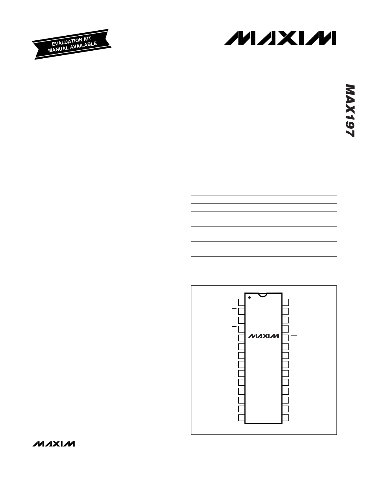
__________________Pin Configuration
TOP VIEW
CLK 1
CS 2
WR 3
RD 4
HBEN 5
SHDN 6
D7 7
D6 8
D5 9
D4 10
D3/D11 11
D2/D10 12
D1/D9 13
D0/D8 14
MAX197
28 DGND
27 VDD
26 REF
25 REFADJ
24 INT
23 CH7
22 CH6
21 CH5
20 CH4
19 CH3
18 CH2
17 CH1
16 CH0
15 AGND
DIP/SO/SSOP/Ceramic SB
________________________________________________________________ Maxim Integrated Products 1
For pricing, delivery, and ordering information, please contact Maxim/Dallas Direct! at
1-888-629-4642, or visit Maxim’s website at www.maxim-ic.com.
1 page 
Multi-Range (±10V, ±5V, +10V, +5V),
Single +5V, 12-Bit DAS with 8+4 Bus Interface
TIMING CHARACTERISTICS
(VDD = 5V ±5%; unipolar/bipolar range; external reference mode, VREF = 4.096V; 4.7µF at REF pin; external clock, fCLK = 2.0MHz
with 50% duty cycle; TA = TMIN to TMAX, unless otherwise noted.)
PARAMETER
CS Pulse Width
WR Pulse Width
CS to WR Setup Time
CS to WR Hold Time
CS to RD Setup Time
CS to RD Hold Time
CLK to WR Setup Time
CLK to WR Hold Time
Data Valid to WR Setup
Data Valid to WR Hold
RD Low to Output Data Valid
HBEN High or HBEN Low to
Output Valid
RD High to Output Disable
RD Low to INT High Delay
SYMBOL
tCS
tWR
tCSWS
tCSWH
tCSRS
tCSRH
tCWS
tCWH
tDS
tDH
tDO
CONDITIONS
Figure 2, CL = 100pF (Note 12)
tDO1 Figure 2, CL = 100pF (Note 12)
tTR
tINT1
(Note 13)
MIN TYP MAX UNITS
80 ns
80 ns
0 ns
0 ns
0 ns
0 ns
100 ns
50 ns
60 ns
0 ns
120 ns
120 ns
70 ns
120 ns
Note 1: Accuracy specifications tested at VDD = 5.0V. Performance at power-supply tolerance limits guaranteed by Power-Supply
Rejection test. Tested for the ±10V input range.
Note 2: External reference: VREF = 4.096V, offset error nulled, ideal last code transition = FS - 3/2LSB.
Note 3: Ground "on" channel; sine wave applied to all "off" channels.
Note 4: Maximum full-power input frequency for 1LSB error with 10ns jitter = 3kHz.
Note 5: Guaranteed by design. Not tested.
Note 6: Use static loads only.
Note 7: Tested using internal reference.
Note 8: PSRR measured at full-scale.
Note 9: External acquisition timing: starts at data valid at ACQMOD = low control byte; ends at rising edge of WR with ACQMOD
= high control byte.
Note 10: Not subject to production testing. Provided for design guidance only.
Note 11: All input control signals specified with tR = tF = 5ns from a voltage level of 0.8V to 2.4V.
Note 12: tDO and tDO1 are measured with the load circuits of Figure 2 and defined as the time required for an output to cross 0.8V
or 2.4V.
Note 13: tTR is defined as the time required for the data lines to change by 0.5V.
_______________________________________________________________________________________ 5
5 Page 
Multi-Range (±10V, ±5V, +10V, +5V),
Single +5V, 12-Bit DAS with 8+4 Bus Interface
tCS
CS
tCSWS
WR
D7–D0
tWR
tDS
CONTROL
BYTE
ACQMOD = "1"
tCSHtAWCQI
tCONV
tDH
CONTROL
BYTE
ACQMOD = "0"
INT
RD
tCSRS
tINT1
tCSRH
HBEN
DOUT
Figure 6. Conversion Timing Using External Acquisition Mode
tD0
tD01
HIGH / LOW
BYTE VALID
HIGH / LOW
BYTE VALID
tTR
How to Read a Conversion
A standard interrupt signal, INT, is provided to allow the
device to flag the µP when the conversion has ended
and a valid result is available. INT goes low when con-
version is complete and the output data is ready
(Figures 5 and 6). It returns high on the first read cycle
or if a new control byte is written.
Clock Modes
The MAX197 operates with either an internal or an
external clock. Control bits (D6, D7) select either inter-
nal or external clock mode. Once the desired clock
mode is selected, changing these bits to program
power-down will not affect the clock mode. In each
mode, internal or external acquisition can be used. At
power-up, external clock mode is selected.
Internal Clock Mode
Select internal clock mode to free the µP from the
burden of running the SAR conversion clock. To select
this mode, write the control byte with D7 = 0 and D6 = 1.
A 100pF capacitor between the CLK pin and ground
sets this frequency to 1.56MHz nominal. Figure 7
shows a linear relationship between the internal clock
period and the value of the external capacitor used.
2000
1500
1000
500
0
0 50 100 150 200 250 300 350
CLOCK PIN CAPACITANCE (pF)
Figure 7. Internal Clock Period vs. Clock Pin Capacitance
______________________________________________________________________________________ 11
11 Page | ||
| Páginas | Total 16 Páginas | |
| PDF Descargar | [ Datasheet MAX197.PDF ] | |
Hoja de datos destacado
| Número de pieza | Descripción | Fabricantes |
| MAX190 | Low-Power / 12-Bit Sampling ADCs with Internal Reference and Power-Down | Maxim Integrated |
| MAX1901 | 500kHz Multi-Output / Low-Noise Power-Supply Controllers for Notebook Computers | Maxim Integrated |
| MAX1901-MAX1904 | 500kHz Multi-Output / Low-Noise Power-Supply Controllers for Notebook Computers | Maxim Integrated |
| MAX1901EAI | 500kHz Multi-Output / Low-Noise Power-Supply Controllers for Notebook Computers | Maxim Integrated |
| Número de pieza | Descripción | Fabricantes |
| SLA6805M | High Voltage 3 phase Motor Driver IC. |
Sanken |
| SDC1742 | 12- and 14-Bit Hybrid Synchro / Resolver-to-Digital Converters. |
Analog Devices |
|
DataSheet.es es una pagina web que funciona como un repositorio de manuales o hoja de datos de muchos de los productos más populares, |
| DataSheet.es | 2020 | Privacy Policy | Contacto | Buscar |