|
|
|
PDF MAX1747 Data sheet ( Hoja de datos )
| Número de pieza | MAX1747 | |
| Descripción | Triple Charge-Pump TFT LCD DC-DC Converter | |
| Fabricantes | Maxim Integrated | |
| Logotipo | ||
Hay una vista previa y un enlace de descarga de MAX1747 (archivo pdf) en la parte inferior de esta página. Total 13 Páginas | ||
|
No Preview Available !
19-1788; Rev 0; 10/00
EVAALVUAAILTAIOBNLEKIT
Triple Charge-Pump TFT LCD
DC-DC Converter
General Description
The MAX1747 triple charge-pump DC-DC converter
provides the regulated voltages required by active
matrix thin-film transistor (TFT) liquid-crystal displays
(LCDs) in a low-profile TSSOP package. One high-
power and two low-power charge pumps convert the
+2.7V to +4.5V input supply voltage into three indepen-
dent output voltages.
The primary high-power charge pump generates an
output voltage (VOUT) between 4.5V and 5.5V that is
regulated within ±1%. The low-power BiCMOS control
circuitry and the low on-resistance (RON) power
MOSFETs maximize efficiency. The adjustable switch-
ing frequency (200kHz to 2MHz) provides fast transient
response and allows the use of small low-profile ceram-
ic capacitors.
The dual low-power charge pumps independently regu-
late one positive output (VPOS) and one negative output
(VNEG). These additional outputs use external diode
and capacitor multiplier stages (as many stages as
required) to regulate output voltages up to +35V and
-35V.
The constant switching frequency and a proprietary
regulation algorithm minimize output ripple and capaci-
tor sizes for all three charge pumps. The MAX1747 is
available in the ultra-thin TSSOP package (1.1mm max
height).
Applications
TFT Active-Matrix LCDs
Passive-Matrix Displays
Personal Digital Assistants (PDAs)
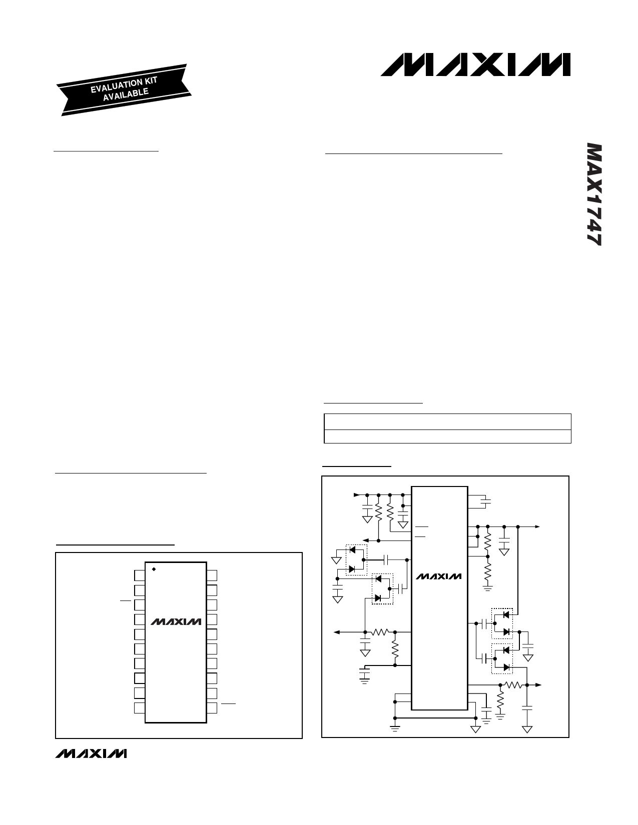
TOP VIEW
TGND 1
TGND 2
RDY 3
FB 4
INTG 5
IN 6
GND 7
REF 8
FBP 9
FBN 10
Pin Configuration
MAX1747
20 OUT
19 CXP
18 SUPM
17 CXN
16 PGND
15 SUPP
14 DRVP
13 SUPN
12 DRVN
11 SHDN
Features
o Adjustable Outputs
Up to +5.5V Main High-Power Output
Up to +35V Positive Charge-Pump Output
Down to -35V Negative Charge-Pump Output
o 200kHz to 2MHz Adjustable Switching Frequency
o +2.7V to +4.5V Input Supply
o Internal Power MOSFETs
o 0.1µA Shutdown Current
o Internal Soft-Start
o Power-Ready Output
o Internal Supply Sequencing
o Fast Transient Response
o Ultra-Thin Solution (No Inductors)
o Thin TSSOP Package (1.1mm max)
Ordering Information
PART
MAX1747EUP
TEMP. RANGE
-40°C to +85°C
PIN-PACKAGE
20 TSSOP
Typical Operating Circuit
INPUT
TO µC
SUPM
IN
SHDN
RDY
DRVN
CXP
CXN
OUT
SUPP
SUPN
FB
MAX1747
MAIN OUTPUT
NEGATIVE
OUTPUT
DRVP
FBN
REF
TGND
GND
FBP
INTG
PGND
POSITIVE
OUTPUT
TSSOP
________________________________________________________________ Maxim Integrated Products 1
For price, delivery, and to place orders, please contact Maxim Distribution at 1-888-629-4642,
or visit Maxim’s website at www.maxim-ic.com.
1 page 
Triple Charge-Pump TFT LCD
DC-DC Converter
ELECTRICAL CHARACTERISTICS (continued)
(VIN = VSUPM = +3.0V, VSUPP = VSUPM = +5V, TGND = PGND = GND, I SHDN = 22µA, COUT = 2 ✕ 4.7µF, CREF = 0.22µF, CINTG =
1500pF, VOUT = +5V, TA = -40°C to +85°C, unless otherwise noted.) (Note 1)
PARAMETER
REFERENCE
Reference Voltage
Reference Undervoltage
Threshold
LOGIC SIGNALS
SHDN Input Low Voltage
SHDN Bias Voltage
SHDN Input Current Range
RDY Output Low Voltage
RDY Output High Leakage
SYMBOL
CONDITIONS
VREF
-2µA < IREF < 50µA
VREF rising
I SHDN
I SHDN = 22µA
For 200kHz to 2MHz operation
ISINK = 2mA
V RDY = 13V
Note 1: Specifications from 0°C to -40°C are guaranteed by design, not production tested.
MIN
1.222
0.95
580
3
MAX UNITS
1.269
1.18
V
V
0.4 V
900 mV
65 µA
0.5 V
1 µA
Typical Operating Characteristics
(Circuit of Figure 1, VIN = VSUPM = +3.3V, TA = +25°C, unless otherwise noted.)
MAIN OUTPUT EFFICIENCY
vs. LOAD CURRENT
(MAIN CHARGE PUMP ONLY)
5.03
5.02 VIN = 3.3V
5.01
5.00
VIN = 2.8V
VIN = 4.0V
4.99
4.98
4.97
0
100 200 300
IOUT (mA)
400
MAIN OUTPUT EFFICIENCY
vs. LOAD CURRENT
(MAIN CHARGE PUMP ONLY)
100
VOUT = 5V
90 VIN = 2.8V
80
VIN = 3.3V
70
VIN = 4.0V
60
50
40
0
100 200 300
IOUT (mA)
400
MAIN OUTPUT EFFICIENCY
vs. LOAD CURRENT
(MAIN CHARGE PUMP ONLY)
100
VOUT = 5V
90 VNEG = -7V WITH INEG = 10mA
VIN = 2.8V VPOS = 12V WITH IPOS = 5mA
80
70 VIN = 3.3V
60
VIN = 4.0V
50
40
0
100 200 300
IOUT (mA)
400
_______________________________________________________________________________________ 5
5 Page 
Triple Charge-Pump TFT LCD
DC-DC Converter
MAX1747
OSC
SUPP
DRVP
C3
VSUPP = 2.7V TO 13V
D1
D2
MAX1747
OSC
IN
SHDN
VON = VIN
RFREQ
CIN
VREF
1.25V
GND
FBP
PGND
R3
R4
VPOS
C4
VPOS = [1 + (R3/R4)] ✕ VREF
VREF = 1.25V
Figure 4. Positive Charge-Pump Block Diagram
GND
RFREQ = kFREQ ✕ (VON - 0.7V)/fOSC
RFREQ IS IN kΩ, kFREQ IS 45.5MHz/mA,
AND fOSC IS IN MHz.
Figure 5. Frequency Adjustment
in the Typical Operating Characteristics). The main out-
put voltage is controlled to be in regulation within 4096
clock cycles (1/fOSC). The negative and positive low-
power charge pumps are controlled to be in regulation
within 2048 clock cycles.
Power-Up Sequencing
Upon power-up or exiting shutdown, the MAX1747
starts a power-up sequence. First, the reference pow-
ers up. Then the primary charge pump powers up with
soft-start enabled. Once the main charge pump reach-
es 90% of its nominal value (VFB > 1.125V), the nega-
tive charge pump turns on. When the negative output
voltage reaches approximately 90% of its nominal value
(VFBN < 125mV), the positive charge pump starts up.
Finally, when the positive output voltage reaches 90%
of its nominal value (VFBP > 1.125V), the active-low
ready signal (RDY) goes low (see Power Ready).
Fault Detection
Once RDY is low, and if any output falls below its fault
detection threshold, RDY goes high impedance.
For the reference, the fault threshold is 1.05V. For the
main charge pump, the fault threshold is 88% of its
nominal value (VFB < 1.1V). For the negative charge
pump, the fault threshold is approximately 88% of its
nominal value (VFBN > 140mV). For the positive charge
pump, the fault threshold is 88% of its nominal value
(VFBP < 1.1V).
Once an output faults, all outputs later in the power
sequence shut down until the faulted output rises
above its power-up threshold. For example, if the nega-
tive charge-pump output voltage falls below the fault-
detection threshold, the main charge pump remains
active while the positive charge pump stops switching
and its output voltage decays, depending on output
capacitance and load. The positive charge-pump out-
put will not power up until the negative charge-pump
output voltage rises above its power-up threshold (see
Power-Up Sequencing).
Power Ready
Power ready is an open-drain output. When the power-
up sequence is properly completed, the MOSFET turns
on and pulls RDY low with a typical 125Ω RON. If a fault
is detected, the internal open-drain MOSFET appears
as a high impedance. Connect a 100kΩ pullup resistor
between RDY and IN for a logic level output.
Voltage Reference
The voltage at REF is nominally 1.25V. The reference
can source up to 50mA with excellent load regulation
(see Typical Operating Characteristics). Connect a
0.22µF bypass capacitor between REF and GND.
During shutdown, the reference is disabled.
Design Procedure
Efficiency Considerations
The efficiency characteristics of the MAX1747 regulat-
ed charge pumps are similar to a linear regulator. They
are dominated by quiescent current at low output cur-
rents and by the input voltage at higher output currents
(see Typical Operating Characteristics). Therefore, the
maximum efficiency may be approximated by:
Efficiency ≅ VOUT / (2 ✕ VSUPM) for the main
charge pump
Efficiency ≅ - VNEG / (VSUPN ✕ N) for the negative
low-power charge pump
______________________________________________________________________________________ 11
11 Page | ||
| Páginas | Total 13 Páginas | |
| PDF Descargar | [ Datasheet MAX1747.PDF ] | |
Hoja de datos destacado
| Número de pieza | Descripción | Fabricantes |
| MAX174 | Complete 12-Bit ADCs | Maxim Integrated |
| MAX1740 | SIM/Smart Card Level Translators in MAX | Maxim Integrated |
| MAX17401 | 1-Phase Quick-PWM Intel IMVP-6/GMCH Controller | Maxim Integrated |
| MAX17409 | 1-Phase Quick-PWM NVIDIA CPU Controller | Maxim Integrated Products |
| Número de pieza | Descripción | Fabricantes |
| SLA6805M | High Voltage 3 phase Motor Driver IC. |
Sanken |
| SDC1742 | 12- and 14-Bit Hybrid Synchro / Resolver-to-Digital Converters. |
Analog Devices |
|
DataSheet.es es una pagina web que funciona como un repositorio de manuales o hoja de datos de muchos de los productos más populares, |
| DataSheet.es | 2020 | Privacy Policy | Contacto | Buscar |