|
|
|
PDF MAX530 Data sheet ( Hoja de datos )
| Número de pieza | MAX530 | |
| Descripción | +5V / Low-Power / Parallel-Input / Voltage-Output / 12-Bit DAC | |
| Fabricantes | Maxim Integrated | |
| Logotipo | ||
Hay una vista previa y un enlace de descarga de MAX530 (archivo pdf) en la parte inferior de esta página. Total 16 Páginas | ||
|
No Preview Available !
19-0168; Rev 3; 7/95
+5V, Low-Power, Parallel-Input,
Voltage-Output, 12-Bit DAC
_______________General Description
The MAX530 is a low-power, 12-bit, voltage-output digi-
tal-to-analog converter (DAC) that uses single +5V or
dual ±5V supplies. This device has an on-chip voltage
reference plus an output buffer amplifier. Operating cur-
rent is only 250µA from a single +5V supply, making it
ideal for portable and battery-powered applications. In
addition, the SSOP (Shrink-Small-Outline-Package) mea-
sures only 0.1 square inches, using less board area than
an 8-pin DIP. 12-bit resolution is achieved through laser
trimming of the DAC, op amp, and reference. No further
adjustments are necessary.
Internal gain-setting resistors can be used to define a
DAC output voltage range of 0V to +2.048V, 0V to
+4.096V, or ±2.048V. Four-quadrant multiplication is pos-
sible without the use of external resistors or op amps. The
parallel logic inputs are double buffered and are compati-
ble with 4-bit, 8-bit, and 16-bit microprocessors. For DACs
with similar features but with a serial data interface, refer
to the MAX531/MAX538/MAX539 data sheet.
________________________Applications
Battery-Powered Data-Conversion Products
Minimum Component-Count Analog Systems
Digital Offset/Gain Adjustment
Industrial Process Control
Arbitrary Function Generators
Automatic Test Equipment
Microprocessor-Controlled Calibration
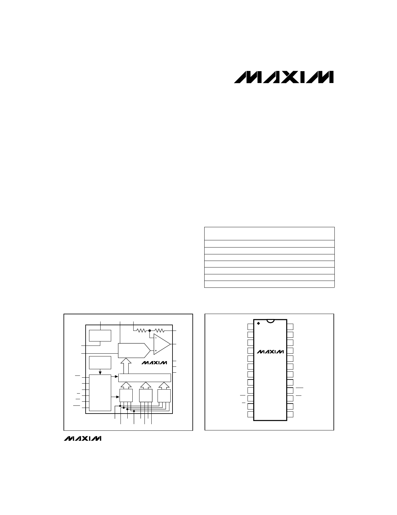
________________Functional Diagram
____________________________Features
o Buffered Voltage Output
o Internal 2.048V Voltage Reference
o Operates from Single +5V or Dual ±5V Supplies
o Low Power Consumption:
250µA Operating Current
40µA Shutdown-Mode Current
o SSOP Package Saves Space
o Relative Accuracy: ±1/2 LSB Max Over
Temperature
o Guaranteed Monotonic Over Temperature
o 4-Quadrant Multiplication with No External
Components
o Power-On Reset
o Double-Buffered Parallel Logic Inputs
______________Ordering Information
PART
TEMP. RANGE
PIN-PACKAGE
ERROR
(LSB)
MAX530ACNG 0°C to +70°C 24 Narrow Plastic DIP ±1/2
MAX530BCNG 0°C to +70°C 24 Narrow Plastic DIP ±1
MAX530ACWG
MAX530BCWG
MAX530ACAG
MAX530BCAG
0°C to +70°C
0°C to +70°C
0°C to +70°C
0°C to +70°C
24 Wide SO
24 Wide SO
24 SSOP
24 SSOP
±1/2
±1
±1/2
±1
MAX530BC/D 0°C to +70°C Dice*
±1
Ordering Information continued on last page.
* Dice are tested at TA = +25°C, DC parameters only.
__________________Pin Configuration
REFGND 17
AGND 14
CLR 15
A0 8
A1 9
CS 11
WR 10
LDAC 16
REFOUT
18
REFIN ROFS
13 22
2.048V
REFERENCE
POWER-ON
RESET
DAC LATCH
MAX530
12-BIT DAC LATCH
21 RFB
20 VOUT
23 VDD
12 DGND
19
VSS
CONTROL
LOGIC
NBL
INPUT
LATCH
NBM
INPUT
LATCH
NBH
INPUT
LATCH
24 1 2 3 4 5 6 7
D0/D8 D2/D10 D4 D6
D1/D9 D3/D11 D5 D7
TOP VIEW
D1/D9 1
D2/D10 2
D3/D11 3
D4 4
D5 5
D6 6
D7 7
A0 8
A1 9
WR 10
CS 11
DGND 12
MAX530
24 D0/D8
23 VDD
22 ROFS
21 RFB
20 VOUT
19 VSS
18 REFOUT
17 REFGND
16 LDAC
15 CLR
14 AGND
13 REFIN
DIP/SO/SSOP
________________________________________________________________ Maxim Integrated Products 1
Call toll free 1-800-998-8800 for free samples or literature.
1 page 
+5V, Low-Power, Parallel-Input,
Voltage-Output, 12-Bit DAC
ELECTRICAL CHARACTERISTICS—Dual ±5V Supplies (continued)
(VDD = 5V ±10%, VSS = -5V ±10%, AGND = DGND = REFGND = 0V, REFIN = 2.048V (external), RFB = ROFS = VOUT,
CREFOUT = 33µF, RL = 10kΩ, CL = 100pF, TA = TMIN to TMAX, unless otherwise noted.)
Note 2: In single supply, INL and GE are calculated from code 11 to code 4095.
Note 3: Zero Code, Bipolar and Gain Error PSRR are input referred specifications. In Unity Gain, the specification is 500µV.
In Gain = 2 and Bipolar modes, the specification is 1mV.
Note 4: Guaranteed by design.
Note 5: REFIN = 1kHz, 2.0Vp-p.
Note 6: For specified performance, VDD = 5V ±10% is guaranteed by PSRR tests.
Note 7: For specified performance, VSS = -5V ±10% is guaranteed by PSRR tests.
Note 8: Tested at IOUT = 100µA. The reference can typically source up to 5mA (see Typical Operating Characteristics).
__________________________________________Typical Operating Characteristics
(TA = +25°C, single supply (+5V), unity gain, code = all 1s, unless otherwise noted).
INTEGRAL NONLINEARITY vs.
DIGITAL INPUT CODE (0–11)
0.25
DUAL
SUPPLIES
0
-0.50
-1.00
SINGLE
SUPPLY
INTEGRAL NONLINEARITY vs.
DIGITAL INPUT CODE (11–4095)
0.25
0
OUTPUT SINK CAPABILITY vs.
OUTPUT PULL-DOWN VOLTAGE
16
14
12
10
8
6
4
2
-1.25
0
2 4 6 8 10 12
DIGITAL INPUT CODE (DECIMAL)
-0.25
11 512 1024 1536 2048 2560 3072 3584 4095
DIGITAL INPUT CODE (DECIMAL)
0
0
0.2 0.4 0.6 0.8 1.0
OUTPUT PULL-DOWN VOLTAGE (V)
OUTPUT SOURCE CAPABILITY vs.
OUTPUT PULL-UP VOLTAGE
8
7
6
5
4
3
2
1
0
0
1 234
OUTPUT PULL-UP VOLTAGE (V)
5
ANALOG FEEDTHROUGH vs.
FREQUENCY
-110
-100
-90
-80
-70 REFIN = 2Vp-p
-60
-50
-40
-30
-20
-10
0
1
CODE = ALL 0s,
DUAL SUPPLIES (±5V)
10 100 1k 10k
FREQUENCY (Hz)
100k
1M
2.055
REFERENCE VOLTAGE vs.
TEMPERATURE
2.050
2.045
-60 -40 -20 0 20 40 60 80 100 120 140
TEMPERATURE (°C)
_______________________________________________________________________________________ 5
5 Page 
+5V, Low-Power, Parallel-Input,
Voltage-Output, 12-Bit DAC
A0-A1
CS
WR
DATA BITS
(8-BIT BYTE OR
4-BIT NIBBLE)
CLR
ADDRESS BUS VALID
VIH
VIL
tAWH
tCWS
tAWS
tWR
tCWH
tDS tDH
VIH
VIL
DATA BUS
VALID
tCLR
LDAC
NOTE:
TIMING
MEASUREMENT REFERENCE LEVEL IS
VIH + VIL
2
tLDAC
Figure 4. MAX530 Write-Cycle Timing Diagram
Parallel Logic Interface
Designed to interface with 4-bit, 8-bit, and 16-bit micro-
processors (µPs), the MAX530 uses 8 data pins and
double-buffered logic inputs to load data as 4 + 4 + 4
or 8 + 4. The 12-bit DAC latch is updated simultane-
ously through the control signal LDAC. Signals A0, A1,
WR, and CS select which input latches to update. The
12-bit data is broken down into nibbles (NB); NBL is
the enable signal for the lowest 4 bits, NBM is the
enable for the middle 4 bits, and NBH is the enable for
the highest and most significant 4 bits. Table 2 lists the
address decoding scheme.
Refer to Figure 4 for the MAX530 write-cycle timing
diagram.
Figure 5 shows the circuit configuration for a 4-bit µP
application. Figure 6 shows the corresponding timing
sequence. The 4 low bits (D0-D3) are connected in paral-
lel to the other 4 bits (D4-D7) and then to the µP bus.
Address lines A0 and A1 enable the input data latches
for the high, middle, or low data nibbles. The µP sends
chip select (CS) and write (WR) signals to latch in each of
three nibbles in three cycles when the data is valid.
Figure 7 shows a typical interface to an 8-bit or a 16-bit
µP. Connect 8 data bits from the data bus to pins D0-D7
on the MAX530. With LDAC held high, the user can load
NBH or NBL + NBM in any order. Figure 8a shows the
corresponding timing sequence. For fastest throughput,
use Figure 8b’s sequence. Address lines A0 and A1 are
tied together and the DAC is loaded in 2 cycles as 8 + 4.
In this scheme, with LDAC held low, the DAC latch is
transparent. Always load NBL and NBM first, followed by
NBH.
LDAC is asynchronous with respect to WR. If LDAC is
brought low before or at the same time WR goes high,
LDAC must remain low for at least 50ns to ensure the cor-
rect data is latched. Data is latched into DAC registers on
LDAC’s rising edge.
______________________________________________________________________________________ 11
11 Page | ||
| Páginas | Total 16 Páginas | |
| PDF Descargar | [ Datasheet MAX530.PDF ] | |
Hoja de datos destacado
| Número de pieza | Descripción | Fabricantes |
| MAX530 | +5V / Low-Power / Parallel-Input / Voltage-Output / 12-Bit DAC | Maxim Integrated |
| MAX5302 | Low-Power / 12-Bit Voltage-Output DAC with Serial Interface | Maxim Integrated |
| MAX5304 | 10-Bit Voltage-Output DAC in 8-Pin MAX | Maxim Integrated |
| MAX5306 | PLASTIC ENCAPSULATED DEVICES | Maxim Integrated |
| Número de pieza | Descripción | Fabricantes |
| SLA6805M | High Voltage 3 phase Motor Driver IC. |
Sanken |
| SDC1742 | 12- and 14-Bit Hybrid Synchro / Resolver-to-Digital Converters. |
Analog Devices |
|
DataSheet.es es una pagina web que funciona como un repositorio de manuales o hoja de datos de muchos de los productos más populares, |
| DataSheet.es | 2020 | Privacy Policy | Contacto | Buscar |