|
|
|
PDF MAX1112 Data sheet ( Hoja de datos )
| Número de pieza | MAX1112 | |
| Descripción | +5V / Low-Power / Multi-Channel / Serial 8-Bit ADCs | |
| Fabricantes | Maxim Integrated | |
| Logotipo | ||
1. MAX1112 Hay una vista previa y un enlace de descarga de MAX1112 (archivo pdf) en la parte inferior de esta página. Total 20 Páginas | ||
|
No Preview Available !
19-1231; Rev 1; 10/98
EVAALVUAAILTAIOBNLEKIT
+5V, Low-Power, Multi-Channel,
Serial 8-Bit ADCs
General Description
The MAX1112/MAX1113 are low-power, 8-bit, 8-chan-
nel analog-to-digital converters (ADCs) that feature an
internal track/hold, voltage reference, clock, and serial
interface. They operate from a single +4.5V to +5.5V
supply and consume only 135µA while sampling at
rates up to 50ksps. The MAX1112’s 8 analog inputs
and the MAX1113’s 4 analog inputs are software-con-
figurable, allowing unipolar/bipolar and single-
ended/differential operation.
Successive-approximation conversions are performed
using either the internal clock or an external serial-inter-
face clock. The full-scale analog input range is deter-
mined by the 4.096V internal reference, or by an
externally applied reference ranging from 1V to VDD.
The 4-wire serial interface is compatible with the SPI™,
QSPI™, and MICROWIRE™ serial-interface standards.
A serial-strobe output provides the end-of-conversion
signal for interrupt-driven processors.
The MAX1112/MAX1113 have a software-program-
mable, 2µA automatic power-down mode to minimize
power consumption. Using power-down, the supply
current is reduced to 13µA at 1ksps, and only 82µA at
10ksps. Power-down can also be controlled using the
SHDN input pin. Accessing the serial interface automat-
ically powers up the device.
The MAX1112 is available in 20-pin SSOP and DIP
packages. The MAX1113 is available in small 16-pin
QSOP and DIP packages.
____________________________Features
o +4.5V to +5.5V Single Supply
o Low Power: 135µA at 50ksps
13µA at 1ksps
o 8-Channel Single-Ended or 4-Channel Differential
Inputs (MAX1112)
o 4-Channel Single-Ended or 2-Channel Differential
Inputs (MAX1113)
o Internal Track/Hold; 50kHz Sampling Rate
o Internal 4.096V Reference
o SPI/QSPI/MICROWIRE-Compatible Serial Interface
o Software-Configurable Unipolar or Bipolar Inputs
o Total Unadjusted Error: ±1LSB (max)
±0.3LSB (typ)
Ordering Information
PART
MAX1112CPP
MAX1112CAP
MAX1112C/D
TEMP. RANGE
0°C to +70°C
0°C to +70°C
0°C to +70°C
PIN-PACKAGE
20 Plastic DIP
20 SSOP
Dice*
*Dice are specified at TA = +25°C, DC parameters only.
Ordering Information continued at end of data sheet.
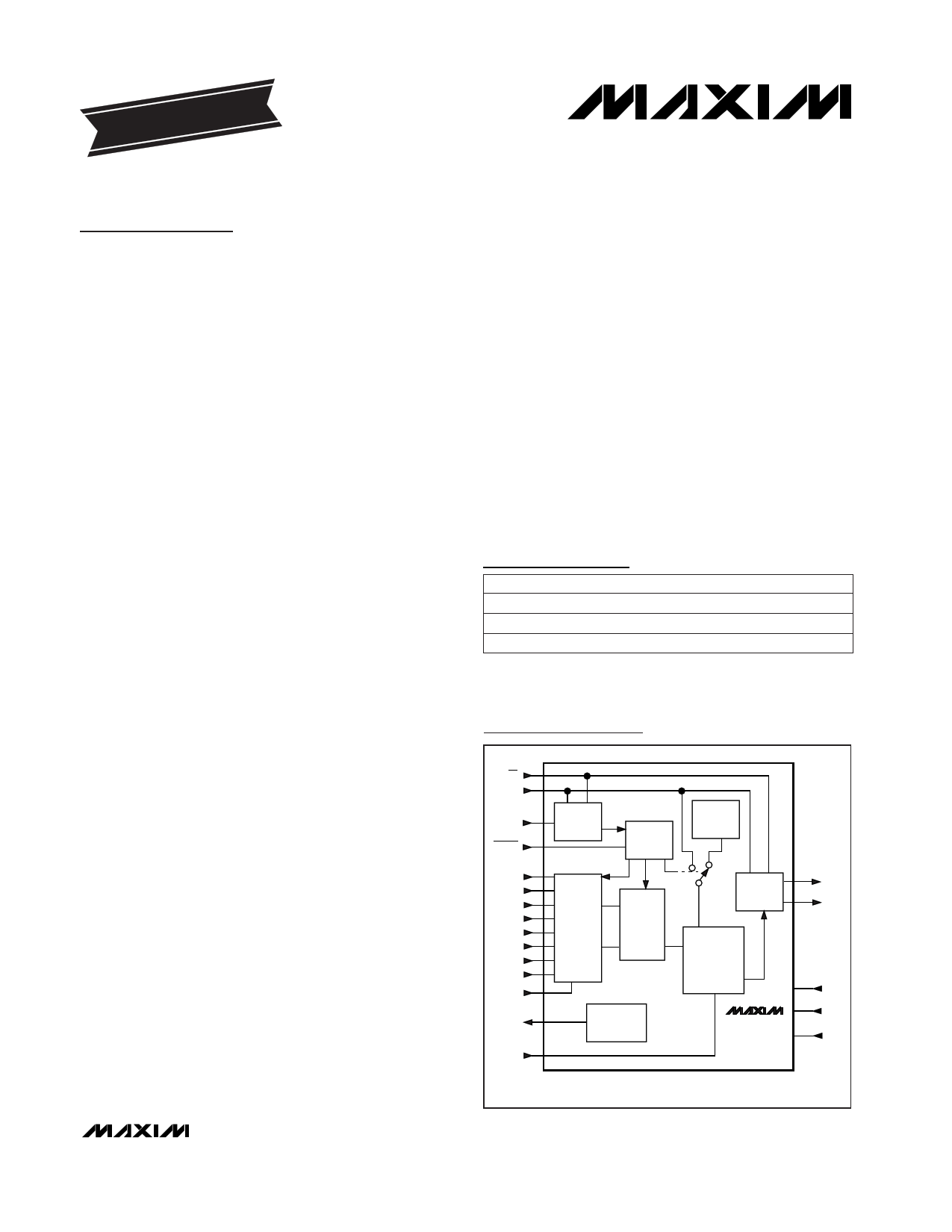
Functional Diagram
________________________Applications
Portable Data Logging
Hand-Held Measurement Devices
Medical Instruments
System Diagnostics
Solar-Powered Remote Systems
4–20mA-Powered Remote
Data-Acquisition Systems
Pin Configurations appear at end of data sheet.
SPI and QSPI are trademarks of Motorola, Inc.
MICROWIRE is a trademark of National Semiconductor Corp.
CS
SCLK
DIN
SHDN
CH0
CH1
CH2
CH3
CH4*
CH5*
CH6*
CH7*
COM
REFOUT
REFIN
INPUT
SHIFT
REGISTER
CONTROL
LOGIC
INT
CLOCK
ANALOG
INPUT
MUX
T/H
+4.096V
REFERENCE
OUTPUT
SHIFT
REGISTER
CLOCK
IN 8-BIT
SAR ADC
OUT
REF
MAX1112
MAX1113
*MAX1112 ONLY
DOUT
SSTRB
VDD
DGND
AGND
________________________________________________________________ Maxim Integrated Products 1
For free samples & the latest literature: http://www.maxim-ic.com, or phone 1-800-998-8800.
For small orders, phone 1-800-835-8769.
1 page 
+5V, Low-Power, Multi-Channel,
Serial 8-Bit ADCs
TIMING CHARACTERISTICS (Figures 8 and 9)
(VDD = +4.5V to +5.5V, TA = TMIN to TMAX, unless otherwise noted.)
PARAMETER
SYMBOL
CONDITIONS
Track/Hold Acquisition Time
DIN to SCLK Setup
DIN to SCLK Hold
SCLK Fall to Output Data Valid
CS Fall to Output Enable
CS Rise to Output Disable
CS to SCLK Rise Setup
CS to SCLK Rise Hold
SCLK Pulse Width High
SCLK Pulse Width Low
SCLK Fall to SSTRB
CS Fall to SSTRB Output Enable
(Note 5)
CS Rise to SSTRB Output
Disable (Note 5)
tACQ
tDS
tDH
tDO
tDV
tTR
tCSS
tCSH
tCH
tCL
tSSTRB
tSDV
tSTR
Figure 1,
CLOAD = 100pF
MAX111_C/E
MAX111_M
Figure 1, CLOAD = 100pF
Figure 2, CLOAD = 100pF
CLOAD = 100pF
Figure 1, external clock mode only,
CLOAD = 100pF
Figure 2, external clock mode only,
CLOAD = 100pF
SSTRB Rise to SCLK Rise
(Note 5)
tSCK Figure 11, internal clock mode only
Wakeup Time
tWAKE
External reference
Internal reference (Note 10)
MIN TYP MAX UNITS
1 µs
100 ns
0 ns
20 200
ns
20 240
240 ns
240 ns
100 ns
0 ns
200 ns
200 ns
240 ns
240 ns
240 ns
0
20
24
ns
µs
ms
Note 1: Relative accuracy is the analog value’s deviation (at any code) from its theoretical value after the full-scale range is calibrated.
Note 2: VREFIN = 4.096V, offset nulled.
Note 3: On-channel grounded; sine wave applied to all off-channels.
Note 4: Conversion time is defined as the number of clock cycles multiplied by the clock period; clock has 50% duty cycle.
Note 5: Guaranteed by design. Not subject to production testing.
Note 6: Common-mode range for the analog inputs is from AGND to VDD.
Note 7: External load should not change during the conversion for specified accuracy.
Note 8: External reference at 4.096V, full-scale input, 500kHz external clock.
Note 9: Measured as | VFS (4.5V) - VFS (5.5V) |.
Note 10: 1µF at REFOUT; internal reference settling to 0.5LSB.
_______________________________________________________________________________________ 5
5 Page 
+5V, Low-Power, Multi-Channel,
Serial 8-Bit ADCs
Table 4. Full-Scale and Zero-Scale Voltages
UNIPOLAR MODE
Full Scale
Zero Scale
VREFIN + COM
COM
Positive
Full Scale
+VREFIN / 2
+ COM
BIPOLAR MODE
Zero
Scale
COM
Negative
Full Scale
-VREFIN / 2
+ COM
in control bytes of $FF (hex), which trigger single-
ended, unipolar conversions on CH7 (MAX1112) or
CH3 (MAX1113) in external clock mode without power-
ing down between conversions. In external clock mode,
the SSTRB output pulses high for two clock periods
before the most significant bit (MSB) of the 8-bit con-
version result is shifted out of DOUT. Varying the ana-
log input alters the output code. A total of 10 clock
cycles is required per conversion. All transitions of the
SSTRB and DOUT outputs occur on SCLK’s falling
edge.
How to Start a Conversion
A conversion is started by clocking a control byte into
DIN. With CS low, each rising edge on SCLK clocks a bit
from DIN into the MAX1112/MAX1113’s internal shift reg-
ister. After CS falls, the first arriving logic “1” bit at DIN
defines the MSB of the control byte. Until this first start bit
arrives, any number of logic “0” bits can be clocked into
DIN with no effect. Table 3 shows the control-byte format.
The MAX1112/MAX1113 are compatible with
MICROWIRE, SPI, and QSPI devices. For SPI, select the
correct clock polarity and sampling edge in the SPI con-
trol registers: set CPOL = 0 and CPHA = 0. MICROWIRE,
SPI, and QSPI all transmit a byte and receive a byte at the
same time. Using the Typical Operating Circuit (Figure 3),
the simplest software interface requires three 8-bit trans-
fers to perform a conversion (one 8-bit transfer to config-
ure the ADC, and two more 8-bit transfers to clock out the
0V TO
+4.096V
ANALOG 0.01µF
INPUT
C1
1µF
VDD
DGND
MAX1112
MAX1113
CH7 (CH3)
AGND
CS
COM
REFOUT
REFIN
SCLK
DIN
SSTRB
DOUT
SHDN
0.1µF
+5V
N.C.
+5V
1µF
500kHz
OSCILLATOR
OSCILLOSCOPE
SCLK
SSTRB
DOUT*
CH1 CH2 CH3 CH4
*FULL-SCALE ANALOG INPUT, CONVERSION RESULT = $FF (HEX)
( ) ARE FOR THE MAX1113.
Figure 5. Quick-Look Circuit
______________________________________________________________________________________ 11
11 Page | ||
| Páginas | Total 20 Páginas | |
| PDF Descargar | [ Datasheet MAX1112.PDF ] | |
Hoja de datos destacado
| Número de pieza | Descripción | Fabricantes |
| MAX111 | Low-Cost / 2-Channel / 14-Bit Serial ADCs | Maxim Integrated |
| MAX1110 | Serial 8-Bit ADCs | Maxim Integrated |
| MAX11100 | 200ksps ADC | Maxim Integrated |
| MAX11101 | 200ksps ADC | Maxim Integrated |
| Número de pieza | Descripción | Fabricantes |
| SLA6805M | High Voltage 3 phase Motor Driver IC. |
Sanken |
| SDC1742 | 12- and 14-Bit Hybrid Synchro / Resolver-to-Digital Converters. |
Analog Devices |
|
DataSheet.es es una pagina web que funciona como un repositorio de manuales o hoja de datos de muchos de los productos más populares, |
| DataSheet.es | 2020 | Privacy Policy | Contacto | Buscar |