|
|
|
PDF PGA204 Data sheet ( Hoja de datos )
| Número de pieza | PGA204 | |
| Descripción | Programmable Gain INSTRUMENTATION AMPLIFIER | |
| Fabricantes | Burr-Brown Corporation | |
| Logotipo | ||
Hay una vista previa y un enlace de descarga de PGA204 (archivo pdf) en la parte inferior de esta página. Total 14 Páginas | ||
|
No Preview Available !
® PGA204
PGA205
Programmable Gain
INSTRUMENTATION AMPLIFIER
FEATURES
q DIGITALLY PROGRAMMABLE GAIN:
PGA204: G=1, 10, 100, 1000V/V
PGA205: G=1, 2, 4, 8V/V
q LOW OFFSET VOLTAGE: 50µV max
q LOW OFFSET VOLTAGE DRIFT: 0.25µV/°C
q LOW INPUT BIAS CURRENT: 2nA max
q LOW QUIESCENT CURRENT: 5.2mA typ
q NO LOGIC SUPPLY REQUIRED
q 16-PIN PLASTIC DIP, SOL-16 PACKAGES
APPLICATIONS
q DATA ACQUISITION SYSTEM
q GENERAL PURPOSE ANALOG BOARDS
q MEDICAL INSTRUMENTATION
DESCRIPTION
The PGA204 and PGA205 are low cost, general pur-
pose programmable-gain instrumentation amplifiers
offering excellent accuracy. Gains are digitally se-
lected: PGA204—1, 10, 100, 1000, and PGA205—1,
2, 4, 8V/V. The precision and versatility, and low cost
of the PGA204 and PGA205 make them ideal for a
wide range of applications.
Gain is selected by two TTL or CMOS-compatible
address lines, A0 and A1. Internal input protection can
withstand up to ±40V on the analog inputs without
damage.
The PGA204 and PGA205 are laser trimmed for very
low offset voltage (50µV), drift (0.25µV/°C) and high
common-mode rejection (115dB at G=1000). They op-
erate with power supplies as low as ±4.5V, allowing use
in battery operated systems. Quiescent current is 5mA.
The PGA204 and PGA205 are available in 16-pin
plastic DIP, and SOL-16 surface-mount packages, speci-
fied for the –40°C to +85°C temperature range.
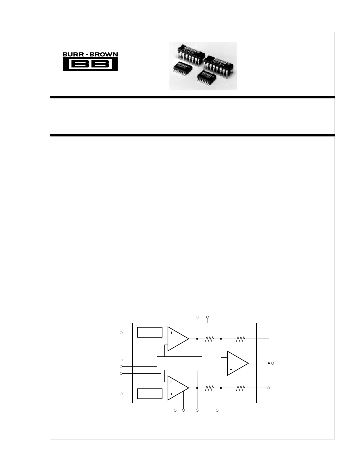
– 4 Over-Voltage
VIN Protection
A1
VO1 V+
1 13
25kΩ
A1
A0
Digital
Ground
16
15
14
Digitally Selected
Feedback Network
+ 5 Over-Voltage
VIN Protection
A2
25kΩ
6 79
8
VOS Adj VO2
V–
PGA204
PGA205 Feedback
25kΩ
12
A3 11 VO
25kΩ
Ref
10
International Airport Industrial Park • Mailing Address: PO Box 11400 • Tucson, AZ 85734 • Street Address: 6730 S. Tucson Blvd. • Tucson, AZ 85706
Tel: (520) 746-1111 • Twx: 910-952-1111 • Cable: BBRCORP • Telex: 066-6491 • FAX: (520) 889-1510 • Immediate Product Info: (800) 548-6132
©1991 Burr-Brown Corporation
PDS1-1176A
PGAP2rin0te4d i/n2U0.S5.A. October, 1993
®
1 page 
DICE INFORMATION
FPO
PGA204/205 DIE TOPOGRAPHY
PIN CONFIGURATION
Top View
VO1 1
NC 2
NC 3
V–IN
V+IN
4
5
VOS Adjust 6
VOS Adjust 7
V– 8
16 A1
15 A0
14 Dig. Ground
13 V+
12 Feedback
11 VO
10 Ref
9 VO2
NC: No Internal Connection.
PAD FUNCTION
PAD FUNCTION
1 VO1
9 VO2
2 — 10 Ref
3 — 11 VO
4 V–IN 12 Feedback
5 V+IN 13 V+
6 VOS Adj 14 Dig. Ground
7 VOS Adj 15
A0
8 V– 16 A1
Substrate Bias: Internally connected to V– power supply.
MECHANICAL INFORMATION
Die Size
Die Thickness
Min. Pad Size
Backing
MILS (0.001")
186 x 130 ±5
20 ±3
4x4
MILLIMETERS
4.72 x 3.30 ±0.13
0.51 ±0.08
0.1 x 0.1
Gold
ELECTROSTATIC
DISCHARGE SENSITIVITY
This integrated circuit can be damaged by ESD. Burr-Brown
recommends that all integrated circuits be handled with ap-
propriate precautions. Failure to observe proper handling and
installation procedures can cause damage.
ESD damage can range from subtle performance degradation
to complete device failure. Precision integrated circuits may
be more susceptible to damage because very small parametric
changes could cause the device not to meet its published
specifications.
®
5 PGA204/205
5 Page 
V+
4 Over-Voltage
– Protection
VIN A1
100kΩ
100kΩ
16
15
14
Digitally Selected
Feedback Network
Switches, jumpers
or open-collector
logic output.
+
VIN
5
Over-Voltage
Protection
A2
Digital ground can
alternatively be connected
to V– power supply.
6 79
VOS
Adj
VO2
FIGURE 2. Switch or Jumper-Selected Digital Inputs.
1.3mA flows in the digital ground pin. It is good practice to
return digital ground through a separate connection path so
that analog ground is not affected by the digital ground
current.
The digital inputs, A0 and A1, are not latched; a change in
logic inputs immediately selects a new gain. Switching time
of the logic is approximately 1µs. The time to respond to
gain change is effectively the time it takes the amplifier to
settle to a new output voltage in the newly selected gain (see
settling time specifications).
Many applications use an external logic latch to access gain
control data from a high speed data bus (see Figure 7). Using
an external latch isolates the high speed digital bus from
sensitive analog circuitry. Locate the latch circuitry as far as
practical from analog circuitry.
Some applications select gain of the PGA204/205 with
switches or jumpers. Figure 2 shows pull-up resistors con-
nected to assure a noise-free logic “1” when the switch,
jumper or open-collector logic is open or off. Fixed-gain
applications can connect the logic inputs directly to V+ or
V– (or other valid logic level); no resistor is required.
OFFSET VOLTAGE
Voltage offset of the PGA204/205 consists of two compo-
nents—input stage offset and output stage offset. Both
components are specified in the specification table in equa-
tion form:
VOS = VOSI + VOSO / G
(1)
where:
VOS total is the combined offset, referred to the input.
VOSI is the offset voltage of the input stage, A1 and A2.
VOSO is the offset voltage of the output difference
amplifier, A3.
VOSI and VOSO do not change with gain. The composite
offset voltage VOS changes with gain because of the gain
term in equation 1. Input stage offset dominates in high gain
(G≥100); both sources of offset may contribute at low gain
(G=1 to 10).
OFFSET TRIMMING
Both the input and output stages are laser trimmed for very
low offset voltage and drift. Many applications require no
external offset adjustment.
Figure 3 shows an optional input offset voltage trim circuit.
This circuit should be used to adjust only the input stage
offset voltage of the PGA204/205. Do this by programming
– 4 Over-Voltage
VIN Protection
A1
VO1 V+
1 13
25kΩ
A1
A0
Digital
Ground
16
15
14
Digitally Selected
Feedback Network
+ 5 Over-Voltage
VIN Protection
A2
25kΩ
6 79
8
Input Offset
Adjustment
Trim Range
≈ ±250µV
VO2
200kΩ
to 1MΩ
V+
V–
FIGURE 3. Optional Offset Voltage Trim Circuit.
PGA204
PGA205 Feedback
25kΩ
12
Resistors can be substituted
for REF200. Power supply
rejection will be degraded.
A3 11 VO = G (VI+N – VI–N) + VREF V+
25kΩ
VREF
10
±10mV
Adjustment Range
OPA177
Output Offset
Adjustment
10kΩ
100µA
1/2 REF200
100Ω
100Ω
100µA
1/2 REF200
V–
11 PGA204/205
®
11 Page | ||
| Páginas | Total 14 Páginas | |
| PDF Descargar | [ Datasheet PGA204.PDF ] | |
Hoja de datos destacado
| Número de pieza | Descripción | Fabricantes |
| PGA200 | Digitally Controlled Programmable-Gain INSTRUMENTATION AMPLIFIER | Burr-Brown Corporation |
| PGA201 | Digitally Controlled Programmable-Gain INSTRUMENTATION AMPLIFIER | Burr-Brown Corporation |
| PGA202 | Digitally Controlled Programmable-Gain INSTRUMENTATION AMPLIFIER | Burr-Brown Corporation |
| PGA202AG | Digitally Controlled Programmable-Gain INSTRUMENTATION AMPLIFIER | Burr-Brown Corporation |
| Número de pieza | Descripción | Fabricantes |
| SLA6805M | High Voltage 3 phase Motor Driver IC. |
Sanken |
| SDC1742 | 12- and 14-Bit Hybrid Synchro / Resolver-to-Digital Converters. |
Analog Devices |
|
DataSheet.es es una pagina web que funciona como un repositorio de manuales o hoja de datos de muchos de los productos más populares, |
| DataSheet.es | 2020 | Privacy Policy | Contacto | Buscar |