|
|
PDF UPD3747D Data sheet ( Hoja de datos )
| Número de pieza | UPD3747D | |
| Descripción | 7400 PIXELS CCD LINEAR IMAGE SENSOR | |
| Fabricantes | NEC | |
| Logotipo |  |
|
Hay una vista previa y un enlace de descarga de UPD3747D (archivo pdf) en la parte inferior de esta página. Total 20 Páginas | ||
|
No Preview Available !
DATA SHEET
MOS INTEGRATED CIRCUIT
µPD3747
7400 PIXELS CCD LINEAR IMAGE SENSOR
The µ PD3747 is a high-speed and high sensitive CCD (Charge Coupled Device) linear image sensor which changes
optical images to electrical signal.
The µ PD3747 is a 2-output type CCD sensor with 2 rows of high-speed charge transfer register, which transfers the
photo signal electrons of 7400 pixels separately in odd and even pixels. And it has reset feed-through level clamp circuits
and voltage amplifiers. Therefore, it is suitable for 600 dpi/A3 high-speed digital copiers, multi-function products and so on.
FEATURES
• Valid photocell : 7400 pixels
• Photocell pitch : 4.7 µ m
• Photocell size : 4.7 × 4.7 µ m2
• Resolution
: 24 dot/mm (600 dpi) A3 (297 × 420 mm) size (shorter side)
• Data rate
: 44 MHz MAX. (22 MHz/1 output)
• Output type
: 2 outputs in phase
• High sensitivity : 19.0 V/lx•s TYP. (Light source: Daylight color fluorescent lamp)
• Low image lag : 1 % MAX.
• Power supply : +12 V
• Drive clock level : CMOS output under 5 V operation
• On-chip circuits : Reset feed-through level clamp circuits
: Voltage amplifiers
ORDERING INFORMATION
Part Number
Package
µ PD3747D
CCD linear image sensor 22-pin ceramic DIP (CERDIP) (10.16 mm (400))
The information in this document is subject to change without notice. Before using this document, please
confirm that this is the latest version.
Not all devices/types available in every country. Please check with local NEC representative for
availability and additional information.
Document No. S14892EJ1V0DS00 (1st edition)
Date Published June 2000 NS CP (K)
Printed in Japan
©
2000
1 page 
µ PD3747
ELECTRICAL CHARACTERISTICS
TA = +25°C, VOD = 12 V, fφ R = 1 MHz, data rate = 2 MHz, storage time = 10 ms, input signal clock = 5 Vp-p,
light source : 3200 K halogen lamp + C-500S (infrared cut filter, t = 1 mm) + HA-50 (heat absorbing filter, t = 3 mm)
Parameter
Saturation voltage
Saturation exposure
Photo response non-uniformity
Average dark signal
Dark signal non-uniformity
Power consumption
Output impedance
Response
Image lag
Offset level Note 1
Output fall delay time Note 2
Register imbalance
Total transfer efficiency
Response peak
Dynamic range
Reset feed-through noise Note 1
Random noise
Shot noise
Symbol
Test Conditions
Vsat
SE Daylight color fluorescent lamp
PRNU VOUT = 500 mV
ADS Light shielding
DSNU Light shielding
PW
ZO
RF Daylight color fluorescent lamp
IL VOUT = 500 mV
VOS
td VOUT = 500 mV
RI VOUT = 500 mV
TTE
VOUT = 1 V, data rate = 44 MHz
DR1
DR2
RFTN
σ bit
σ line
σ shot
Vsat/DSNU
Vsat/σ bit
Light shielding
Light shielding, bit clamp mode
Light shielding, line clamp mode
VOUT = 500 mV, bit clamp mode
MIN.
1.5
−
−
−
−
−
−
13.3
−
3.7
−
0
94
−
−
−
−300
−
−
−
TYP.
2.0
0.10
5
0.5
8.0
350
0.2
19.0
0.5
4.7
14
1.0
98
550
250
1000
+300
2.0
8.0
8.0
MAX.
−
−
10
3.0
14.0
600
0.3
24.7
1.0
5.7
−
4.0
−
−
−
−
+900
−
−
−
Unit
V
lx•s
%
mV
mV
mW
kΩ
V/lx•s
%
V
ns
%
%
nm
times
times
mV
mV
mV
mV
Notes 1. Refer to TIMING CHART 2, 3.
2. When the fall time of φ 2L (t2’) is the TYP. value (refer to TIMING CHART 2, 3). Note that VOUT1 and VOUT2 are
the outputs of the two steps of emitter-follower shown in APPLICATION CIRCUIT EXAMPLE.
Data Sheet S14892EJ1V0DS00
5
5 Page 
µ PD3747
DEFINITIONS OF CHARACTERISTIC ITEMS
1. Saturation voltage : Vsat
Output signal voltage at which the response linearity is lost.
2. Saturation exposure : SE
Product of intensity of illumination (lx) and storage time (s) when saturation of output voltage occurs.
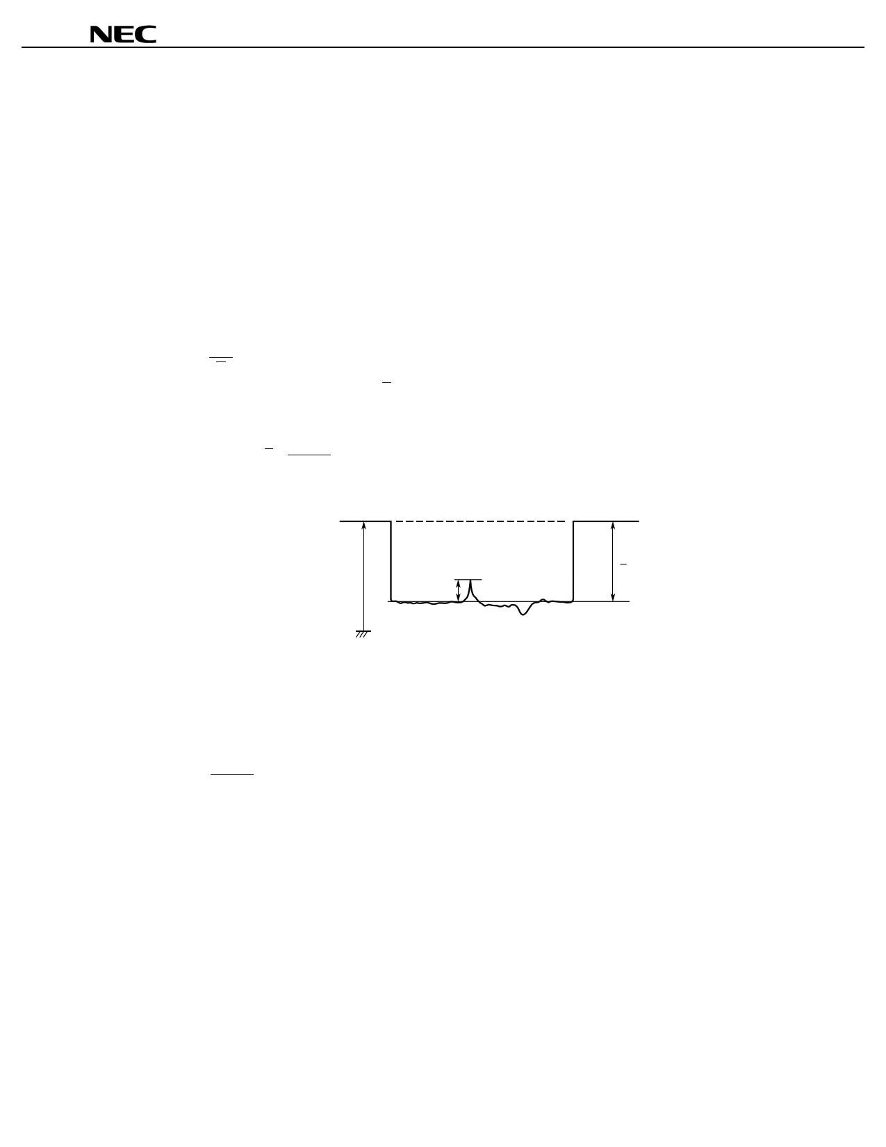
3. Photo response non-uniformity : PRNU
The output signal non-uniformity of all the valid pixels when the photosensitive surface is applied with the light of
uniform illumination. This is calculated by the following formula.
PRNU (%) = ∆x × 100
x
∆x: maximum of xj − x
7400
Σ xj
j=1
x=
7400
xj: Output voltage of valid pixel number j
VOUT
Register dark
DC level
∆x
x
4. Average dark signal : ADS
Average output signal voltage of all the valid pixels at light shielding. This is calculated by the following formula.
ADS (mV) =
7400
Σ dj
j=1
7400
dj: Dark signal of valid pixel number j
Data Sheet S14892EJ1V0DS00
11
11 Page | ||
| Páginas | Total 20 Páginas | |
| PDF Descargar | [ Datasheet UPD3747D.PDF ] | |
Hoja de datos destacado
| Número de pieza | Descripción | Fabricantes |
| UPD3747 | 7400 PIXELS CCD LINEAR IMAGE SENSOR | NEC |
| UPD3747D | 7400 PIXELS CCD LINEAR IMAGE SENSOR | NEC |
| Número de pieza | Descripción | Fabricantes |
| SLA6805M | High Voltage 3 phase Motor Driver IC. |
Sanken |
| SDC1742 | 12- and 14-Bit Hybrid Synchro / Resolver-to-Digital Converters. |
Analog Devices |
|
DataSheet.es es una pagina web que funciona como un repositorio de manuales o hoja de datos de muchos de los productos más populares, |
| DataSheet.es | 2020 | Privacy Policy | Contacto | Buscar |
