No Preview Available !

Order this document by TL494/D
SWITCHMODE™ Pulse Width
Modulation Control Circuit
The TL494 is a fixed frequency, pulse width modulation control circuit
designed primarily for SWITCHMODE power supply control.
• Complete Pulse Width Modulation Control Circuitry
• On–Chip Oscillator with Master or Slave Operation
• On–Chip Error Amplifiers
• On–Chip 5.0 V Reference
• Adjustable Deadtime Control
• Uncommitted Output Transistors Rated to 500 mA Source or Sink
• Output Control for Push–Pull or Single–Ended Operation
• Undervoltage Lockout
TL494
SWITCHMODE
PULSE WIDTH MODULATION
CONTROL CIRCUIT
SEMICONDUCTOR
TECHNICAL DATA
D SUFFIX
PLASTIC PACKAGE
CASE 751B
(SO–16)
N SUFFIX
PLASTIC PACKAGE
CASE 648
PIN CONNECTIONS
MAXIMUM RATINGS (Full operating ambient temperature range applies,
unless otherwise noted.)
Rating
Symbol TL494C TL494I Unit
Power Supply Voltage
Collector Output Voltage
Collector Output Current
(Each transistor) (Note 1)
VCC
VC1,
VC2
IC1, IC2
42
42
500
V
V
mA
Amplifier Input Voltage Range
Power Dissipation @ TA ≤ 45°C
Thermal Resistance,
Junction–to–Ambient
VIR
PD
RθJA
–0.3 to +42
1000
80
V
mW
°C/W
Operating Junction Temperature
Storage Temperature Range
Operating Ambient Temperature Range
TL494C
TL494I
TJ
Tstg
TA
125
–55 to +125
0 to +70
– 25 to +85
°C
°C
°C
Derating Ambient Temperature
TA
NOTE: 1. Maximum thermal limits must be observed.
45 °C
Noninv
Input
1
Inv
Input
2
+
Error
–Amp
1
Compen/PWN
Comp Input
3
Deadtime
Control
4
≈ 0.1 V
+
2
Error
Amp–
VCC
5.0 V
REF
16
Noninv
Input
15
Inv
Input
14 Vref
13
Output
Control
CT 5
RT 6
Ground 7
Oscillator
12 VCC
11 C2
Q2
10 E2
C1 8
Q1
9 E1
(Top View)
ORDERING INFORMATION
Device
Operating
Temperature Range
Package
TL494CD
TL494CN
TA = 0° to +70°C
SO–16
Plastic
TL494IN TA = – 25° to +85°C
Plastic
MOTOROLA ANALOG IC DEVICE DATA
© Motorola, Inc. 1996
Rev 1
1

TL494
APPLICATIONS INFORMATION
Description
The TL494 is a fixed–frequency pulse width modulation
control circuit, incorporating the primary building blocks
required for the control of a switching power supply. (See
Figure 1.) An internal–linear sawtooth oscillator is frequency–
programmable by two external components, RT and CT. The
approximate oscillator frequency is determined by:
fosc ≈
1.1
RT • CT
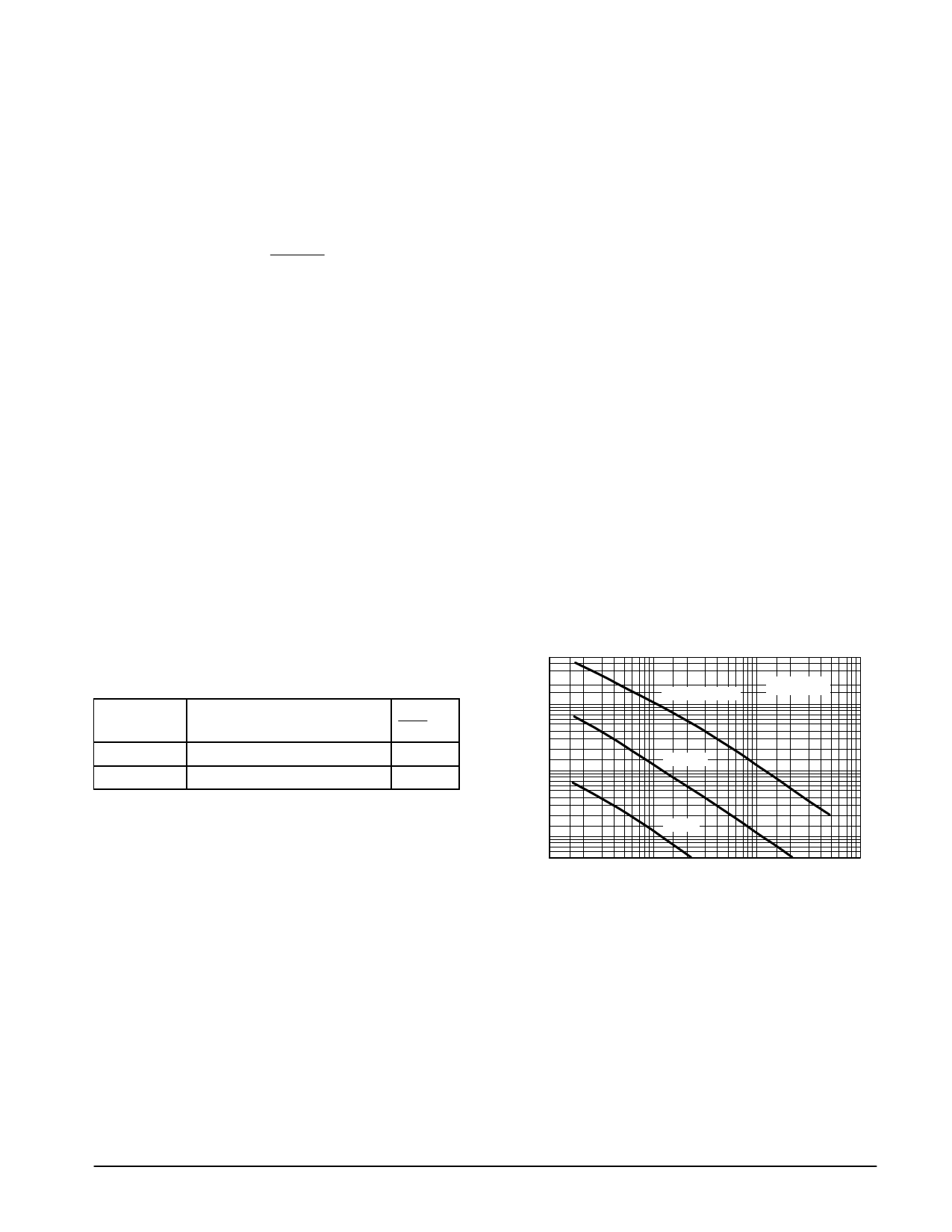
For more information refer to Figure 3.
Output pulse width modulation is accomplished by
comparison of the positive sawtooth waveform across
capacitor CT to either of two control signals. The NOR gates,
which drive output transistors Q1 and Q2, are enabled only
when the flip–flop clock–input line is in its low state. This
happens only during that portion of time when the sawtooth
voltage is greater than the control signals. Therefore, an
increase in control–signal amplitude causes a corresponding
linear decrease of output pulse width. (Refer to the Timing
Diagram shown in Figure 2.)
The control signals are external inputs that can be fed into
the deadtime control, the error amplifier inputs, or the
feedback input. The deadtime control comparator has an
effective 120 mV input offset which limits the minimum output
deadtime to approximately the first 4% of the sawtooth–cycle
time. This would result in a maximum duty cycle on a given
output of 96% with the output control grounded, and 48% with
it connected to the reference line. Additional deadtime may
be imposed on the output by setting the deadtime–control
input to a fixed voltage, ranging between 0 V to 3.3 V.
may be used to sense power–supply output voltage and
current. The error–amplifier outputs are active high and are
ORed together at the noninverting input of the pulse–width
modulator comparator. With this configuration, the amplifier
that demands minimum output on time, dominates control of
the loop.
When capacitor CT is discharged, a positive pulse is
generated on the output of the deadtime comparator, which
clocks the pulse–steering flip–flop and inhibits the output
transistors, Q1 and Q2. With the output–control connected to
the reference line, the pulse–steering flip–flop directs the
modulated pulses to each of the two output transistors
alternately for push–pull operation. The output frequency is
equal to half that of the oscillator. Output drive can also be
taken from Q1 or Q2, when single–ended operation with a
maximum on–time of less than 50% is required. This is
desirable when the output transformer has a ringback
winding with a catch diode used for snubbing. When higher
output–drive currents are required for single–ended
operation, Q1 and Q2 may be connected in parallel, and the
output–mode pin must be tied to ground to disable the
flip–flop. The output frequency will now be equal to that of the
oscillator.
The TL494 has an internal 5.0 V reference capable of
sourcing up to 10 mA of load current for external bias circuits.
The reference has an internal accuracy of ±5.0% with a
typical thermal drift of less than 50 mV over an operating
temperature range of 0° to 70°C.
Figure 3. Oscillator Frequency versus
Timing Resistance
500 k
Functional Table
Input/Output
Controls
Output Function
Grounded Single–ended PWM @ Q1 and Q2
fout
fosc
=
1.0
@ Vref Push–pull Operation
0.5
100 k
10 k
CT = 0.001 µF
VCC = 15 V
0.01 µF
The pulse width modulator comparator provides a means
for the error amplifiers to adjust the output pulse width from
the maximum percent on–time, established by the deadtime
control input, down to zero, as the voltage at the feedback pin
varies from 0.5 V to 3.5 V. Both error amplifiers have a
common mode input range from –0.3 V to (VCC – 2V), and
0.1 µF
1.0 k
500
1.0 k 2.0 k 5.0 k 10 k 20 k 50 k 100 k 200 k
RT, TIMING RESISTANCE (Ω)
500 k 1.0 M
MOTOROLA ANALOG IC DEVICE DATA
5

–A–
16
1
H
G
9
B
8
TL494
OUTLINE DIMENSIONS
N SUFFIX
PLASTIC PACKAGE
CASE 648–08
ISSUE R
FC
S
L
–T–
SEATING
PLANE
KJ
D 16 PL
0.25 (0.010) M T A M
M
NOTES:
1. DIMENSIONING AND TOLERANCING PER ANSI
Y14.5M, 1982.
2. CONTROLLING DIMENSION: INCH.
3. DIMENSION L TO CENTER OF LEADS WHEN
FORMED PARALLEL.
4. DIMENSION B DOES NOT INCLUDE MOLD FLASH.
5. ROUNDED CORNERS OPTIONAL.
INCHES
MILLIMETERS
DIM MIN MAX MIN MAX
A 0.740 0.770 18.80 19.55
B 0.250 0.270 6.35 6.85
C 0.145 0.175 3.69 4.44
D 0.015 0.021 0.39 0.53
F 0.040 0.70 1.02 1.77
G 0.100 BSC
2.54 BSC
H 0.050 BSC
1.27 BSC
J 0.008 0.015 0.21 0.38
K 0.110 0.130 2.80 3.30
L 0.295 0.305 7.50 7.74
M 0_ 10_ 0 _ 10 _
S 0.020 0.040 0.51 1.01
–A–
16
1
D SUFFIX
PLASTIC PACKAGE
CASE 751B–05
(SO–16)
ISSUE J
9
–B– P 8 PL
8 0.25 (0.010) M B S
G
–T– SEATING
PLANE
K
C
D 16 PL
0.25 (0.010) M T B S A S
R X 45_
F
MJ
NOTES:
1. DIMENSIONING AND TOLERANCING PER
ANSI Y14.5M, 1982.
2. CONTROLLING DIMENSION: MILLIMETER.
3. DIMENSIONS A AND B DO NOT INCLUDE
MOLD PROTRUSION.
4. MAXIMUM MOLD PROTRUSION 0.15 (0.006)
PER SIDE.
5. DIMENSION D DOES NOT INCLUDE DAMBAR
PROTRUSION. ALLOWABLE DAMBAR
PROTRUSION SHALL BE 0.127 (0.005) TOTAL
IN EXCESS OF THE D DIMENSION AT
MAXIMUM MATERIAL CONDITION.
MILLIMETERS
INCHES
DIM MIN MAX MIN MAX
A 9.80 10.00 0.386 0.393
B 3.80 4.00 0.150 0.157
C 1.35 1.75 0.054 0.068
D 0.35 0.49 0.014 0.019
F 0.40 1.25 0.016 0.049
G 1.27 BSC
0.050 BSC
J 0.19 0.25 0.008 0.009
K 0.10 0.25 0.004 0.009
M 0_ 7_ 0_ 7_
P 5.80 6.20 0.229 0.244
R 0.25 0.50 0.010 0.019
MOTOROLA ANALOG IC DEVICE DATA
11


