|
|
|
PDF X25640 Data sheet ( Hoja de datos )
| Número de pieza | X25640 | |
| Descripción | Advanced SPI Serial E2PROM With Block LockTM Protection | |
| Fabricantes | Xicor | |
| Logotipo | ||
Hay una vista previa y un enlace de descarga de X25640 (archivo pdf) en la parte inferior de esta página. Total 14 Páginas | ||
|
No Preview Available !
APPLICATION NOTES
AVA I L A B L E
X25640AN19 • AN38 • AN41 • AN61
64K
X25640
8K x 8 Bit
Advanced SPI Serial E2PROM With Block LockTM Protection
FEATURES
• 1MHz Clock Rate
• Low Power CMOS
—200µA Standby Current
—5mA Active Current
• 5 Volt Power Supply
• SPI Modes (0,0 & 1,1)
• 8K X 8 Bits
—32 Byte Page Mode
• Block Lock Protection
—Protect 1/4, 1/2 or all of E2PROM Array
• Built-in Inadvertent Write Protection
—Power-Up/Power-Down protection circuitry
—Write Enable Latch
—Write Protect Pin
• Self-Timed Write Cycle
—5ms Write Cycle Time (Typical)
• High Reliability
—Endurance: 100,000 cycles
—Data Retention: 100 Years
—ESD protection: 2000V on all pins
• 8-Lead PDlP Package
• 14-Lead SOIC Package
DESCRIPTION
The X25640 is a CMOS 65,536-bit serial E2PROM,
internally organized as 8K x 8. The X25640 features a
Serial Peripheral Interface (SPI) and software protocol
allowing operation on a simple three-wire bus. The bus
signals are a clock input (SCK) plus separate data in (SI)
and data out (SO) lines. Access to the device is con-
trolled through a chip select (CS) input, allowing any
number of devices to share the same bus.
The X25640 also features two additional inputs that
provide the end user with added flexibility. By asserting
the HOLD input, the X25640 will ignore transitions on its
inputs, thus allowing the host to service higher priority
interrupts. The WP input can be used as a hardwire input
to the X25640 disabling all write attempts to the status
register, thus providing a mechanism for limiting end
user capability of altering 0, 1/4, 1/2 or all of the memory.
The X25640 utilizes Xicor’s proprietary Direct Write™
cell, providing a minimum endurance of 100,000 cycles
and a minimum data retention of 100 years.
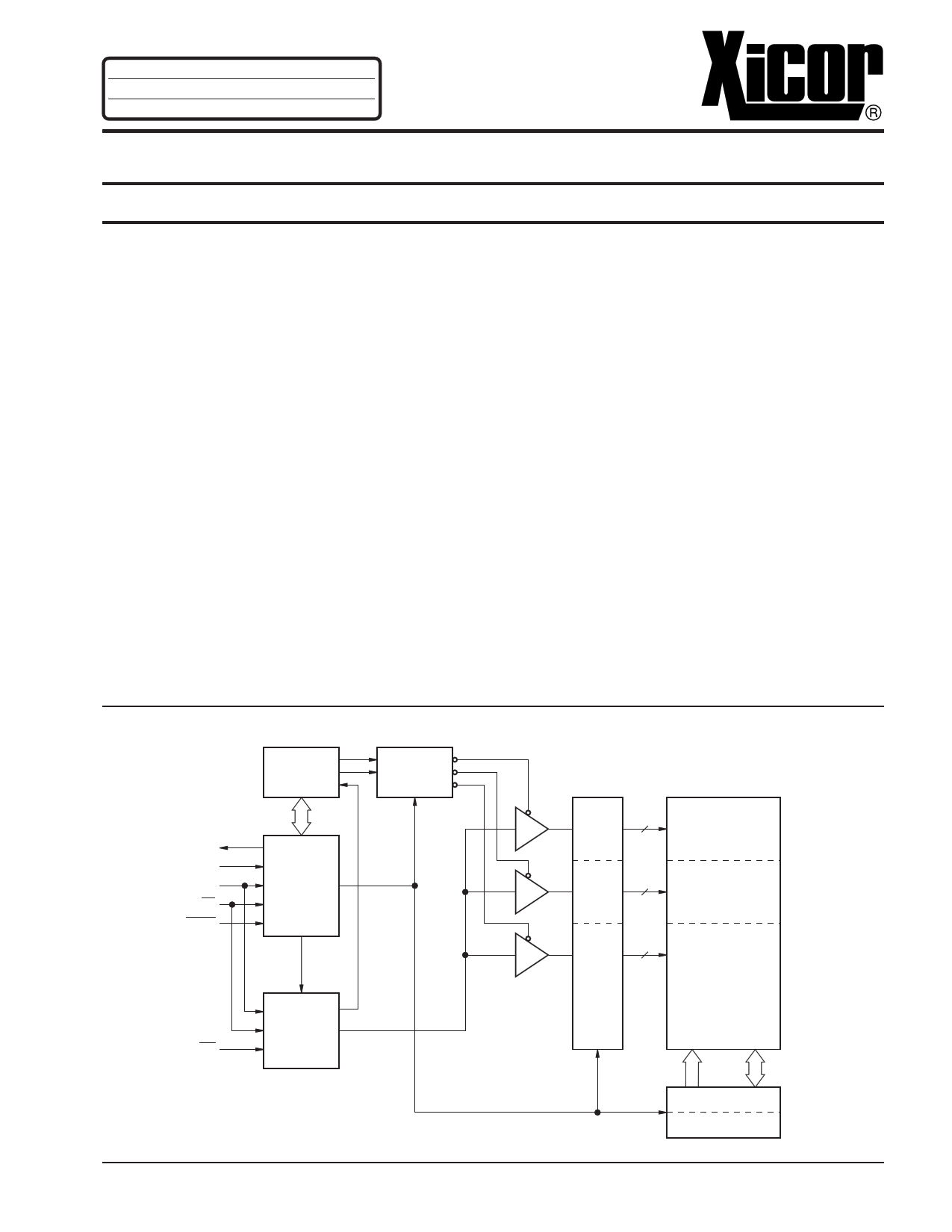
FUNCTIONAL DIAGRAM
SO
SI
SCK
CS
HOLD
STATUS
REGISTER
COMMAND
DECODE
AND
CONTROL
LOGIC
WRITE
PROTECT
LOGIC
X DECODE
LOGIC
64
64
128
8K BYTE
ARRAY
64 X 256
64 X 256
128 X 256
WRITE
CONTROL
AND
WP
TIMING
LOGIC
Direct Write™ and Block Lock™ Protection is a trademark of Xicor, Inc.
©Xicor, Inc. 1994, 1995, 1996 Patents Pending
3089-1.8 6/17/96 T4/C4/D1 NS
1
32 8
Y DECODE
DATA REGISTER
3089 ILL F01
Characteristics subject to change without notice
1 page 
X25640
Operational Notes
The X25640 powers-up in the following state:
• The device is in the low power standby state.
• A HIGH to LOW transition on CS is required to
enter an active state and receive an instruction.
• SO pin is high impedance.
• The “write enable” latch is reset.
Data Protection
The following circuitry has been included to prevent
inadvertent writes:
• The “write enable” latch is reset upon power-up.
• A WREN instruction must be issued to set the “write
enable” latch.
• CS must come HIGH at the proper clock count in
order to start a write cycle.
Figure 1. Read E2PROM Array Operation Sequence
CS
SCK
0 1 2 3 4 5 6 7 8 9 10
20 21 22 23 24 25 26 27 28 29 30
INSTRUCTION
16 BIT ADDRESS
SI
15 14 13
3210
HIGH IMPEDANCE
SO
76
MSB
DATA OUT
543210
3089 ILL F03.1
Figure 2. Read Status Register Operation Sequence
CS
SCK
0 1 2 3 4 5 6 7 8 9 10 11 12 13 14
INSTRUCTION
SI
HIGH IMPEDANCE
SO
76
MSB
DATA OUT
543210
3089 ILL F09.1
5
5 Page 
X25640
Hold Timing
CS
SCK
SO
SI
HOLD
tHD
tHZ
tCD tCD
tHD
tLZ
3089 ILL F12.1
11
11 Page | ||
| Páginas | Total 14 Páginas | |
| PDF Descargar | [ Datasheet X25640.PDF ] | |
Hoja de datos destacado
| Número de pieza | Descripción | Fabricantes |
| X25640 | Advanced SPI Serial E2PROM With Block LockTM Protection | Xicor |
| X25642 | Advanced SPI Serial E 2 PROM with Block Lock TM Protection | Xicor |
| X25642P | Advanced SPI Serial E 2 PROM with Block Lock TM Protection | Xicor |
| X25642P-2.7 | Advanced SPI Serial E 2 PROM with Block Lock TM Protection | Xicor |
| Número de pieza | Descripción | Fabricantes |
| SLA6805M | High Voltage 3 phase Motor Driver IC. |
Sanken |
| SDC1742 | 12- and 14-Bit Hybrid Synchro / Resolver-to-Digital Converters. |
Analog Devices |
|
DataSheet.es es una pagina web que funciona como un repositorio de manuales o hoja de datos de muchos de los productos más populares, |
| DataSheet.es | 2020 | Privacy Policy | Contacto | Buscar |