|
|
|
PDF XC95144XV Data sheet ( Hoja de datos )
| Número de pieza | XC95144XV | |
| Descripción | High-Performance CPLD | |
| Fabricantes | Xilinx | |
| Logotipo | ||
Hay una vista previa y un enlace de descarga de XC95144XV (archivo pdf) en la parte inferior de esta página. Total 9 Páginas | ||
|
No Preview Available !
R
DS051 (v2.2) August 27, 2001
0
XC95144XV High-Performance
CPLD
0 1 Advance Product Specification
Features
• 144 macrocells with 3,200 usable gates
• Available in small footprint packages
- 100-pin TQFP (81 user I/O pins)
- 144-pin TQFP (117 user I/O pins)
- 144-pin CSP (117 user I/O pins)
• Optimized for high-performance 2.5V systems
- Low power operation
- Multi-voltage operation
• Advanced system features
- In-system programmable
- Two separate output banks
- Superior pin-locking and routability with
FastCONNECT II™ switch matrix
- Extra wide 54-input Function Blocks
- Up to 90 product-terms per macrocell with
individual product-term allocation
- Local clock inversion with three global and one
product-term clocks
- Individual output enable per output pin
- Input hysteresis on all user and boundary-scan pin
inputs
- Bus-hold ciruitry on all user pin inputs
- Full IEEE Standard 1149.1 boundary-scan (JTAG)
• Fast concurrent programming
• Slew rate control on individual outputs
• Enhanced data security features
• Excellent quality and reliability
- Endurance exceeding 10,000 program/erase
cycles
- 20 year data retention
- ESD protection exceeding 2,000V
Description
The XC95144XV is a 2.5V CPLD targeted for high-perfor-
mance, low-voltage applications in leading-edge communi-
cations and computing systems. It is comprised of eight
54V18 Function Blocks, providing 3,200 usable gates with
propagation delays of 4 ns.
Power Estimation
Power dissipation in CPLDs can vary substantially depend-
ing on the system frequency, design application and output
loading. To help reduce power dissipation, each macrocell
in a XC9500XV device may be configured for low-power
mode (from the default high-performance mode). In addi-
tion, unused product-terms and macrocells are automati-
cally deactivated by the software to further conserve power.
For a general estimate of ICC, the following equation may be
used:
ICC (mA) =
MCHP(0.36) + MCLP(0.23) + MC(0.005 mA/MHz) f
Where:
MCHP = Macrocells in high-performance (default) mode
MCLP = Macrocells in low-power mode
MC = Total number of macrocells used
f = Clock frequency (MHz)
This calculation is based on typical operating conditions
using a pattern of 16-bit up/down counters in each Function
Block with no output loading. The actual ICC value varies
with the design application and should be verified during
normal system operation.
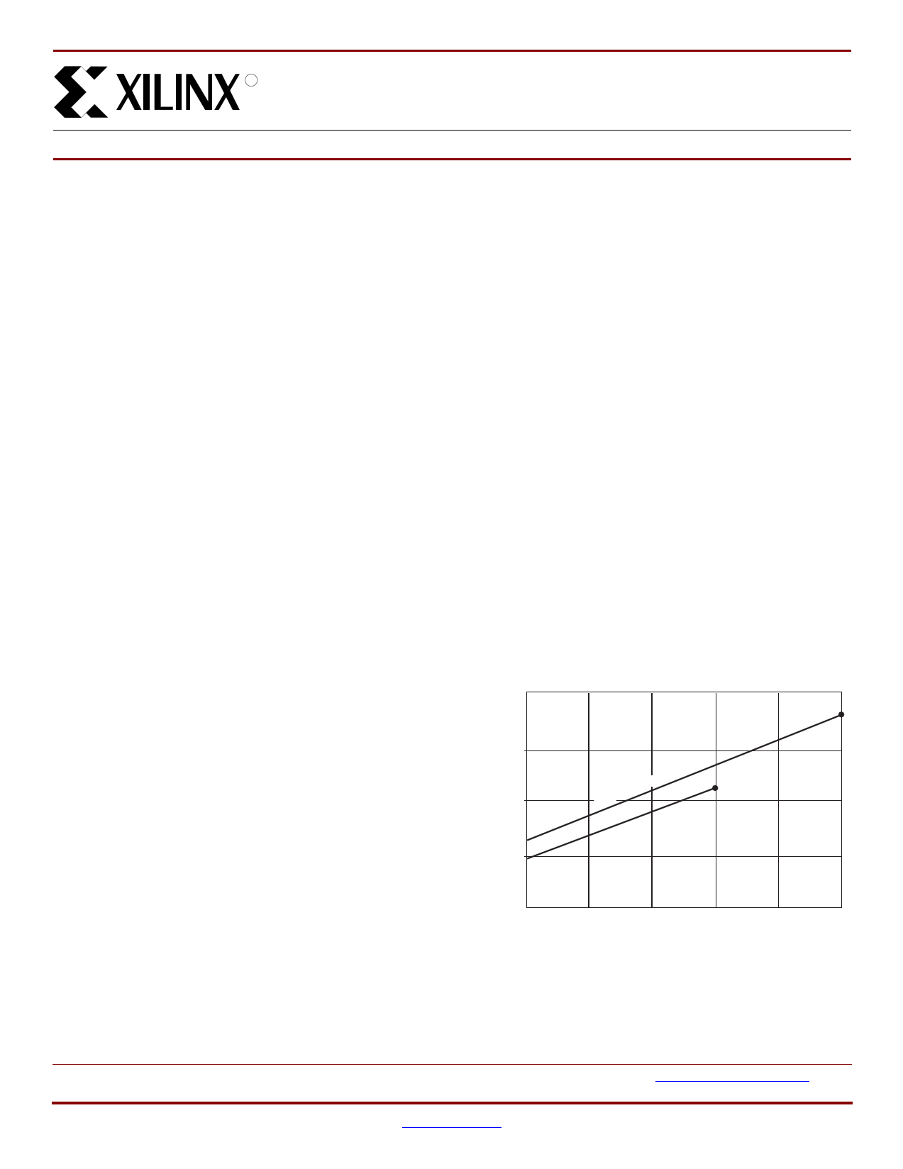
Figure 1 shows the above estimation in a graphical form.
200
200 MHz
150
100 High PLeorfwormPaonwceer
50
120 MHz
0 40 80 120 160 200
Clock Frequency (MHz)
DS051_01_012501
Figure 1: Typical ICC vs. Frequency for XC95144XV
© 2001 Xilinx, Inc. All rights reserved. All Xilinx trademarks, registered trademarks, patents, and disclaimers are as listed at http://www.xilinx.com/legal.htm.
All other trademarks and registered trademarks are the property of their respective owners. All specifications are subject to change without notice.
DS051 (v2.2) August 27, 2001
Advance Product Specification
www.xilinx.com
1-800-255-7778
1
1 page 
R XC95144XV High-Performance CPLD
VTEST
Device Output
R1
Output Type VCCIO
VTEST
R1
R2 CL
3.3V
3.3V
320Ω
360Ω
35 pF
R2 CL
2.5V
1.8V
2.5V
1.8V
250Ω
10KΩ
660Ω
14KΩ
35 pF
35 pF
DS051_03_0601000
Internal Timing Parameters
Figure 3: AC Load Circuit
XC95144XV-4
Symbol
Parameter
Min Max
Buffer Delays
TIN Input buffer delay
TGCK
GCK buffer delay
TGSR
GSR buffer delay
TGTS
GTS buffer delay
TOUT
Output buffer delay
TEN Output buffer enable/disable delay
Product Term Control Delays
- 1.6
- 1.0
- 1.6
- 3.2
- 1.6
-0
TPTCK Product term clock delay
TPTSR Product term set/reset delay
TPTTS Product term 3-state delay
Internal Register and Combinatorial Delays
- 1.4
- 0.6
- 4.0
TPDI
Combinatorial logic propagation delay
TSUI
Register setup time
THI Register hold time
TECSU Register clock enable setup time
TECHO Register clock enable hold time
TCOI
Register clock to output valid time
TAOI Register async. S/R to output delay
TRAI
Register async. S/R recover before clock
TLOGI Internal logic delay
TLOGILP Internal low power logic delay
Feedback Delays
-
1.6
1.2
1.6
1.2
-
-
4.0
-
-
0.2
-
-
-
-
0.2
4.7
0.6
5.6
TF FastCONNECT II™ feedback delay
Time Adders
- 1.6
TPTA
TPTA2
TSLEW
Incremental product term allocator delay
Adjacent macrocell p-term allocator delay
Slew-rate limited delay
- 0.6
- 0.2
- 3.0
Advance Information
Notes:
1. Please contact Xilinx for up-to-date information on advance specifications.
XC95144XV-5 XC95144XV-7
Min Max Min Max
- 2.0 - 2.3
- 1.2 - 1.5
- 2.0 - 3.1
- 4.0 - 5.0
- 2.1 - 2.5
-0-0
- 1.7 - 2.4
- 0.7 - 1.4
- 5.0 - 7.2
- 0.2 - 1.3
2.0 - 2.6 -
1.5 - 2.2 -
2.0 - 2.6 -
1.5 - 2.2 -
- 0.2 - 0.5
- 5.9 - 6.4
5.0 7.5
- 0.7 - 1.4
- 5.7 - 6.4
- 1.6 - 3.5
- 0.7 - 0.8
- 0.3 - 0.3
- 3.0 - 4.0
Preliminary Information
Units
ns
ns
ns
ns
ns
ns
ns
ns
ns
ns
ns
ns
ns
ns
ns
ns
ns
ns
ns
ns
ns
ns
ns
DS051 (v2.2) August 27, 2001
Advance Product Specification
www.xilinx.com
1-800-255-7778
5
5 Page | ||
| Páginas | Total 9 Páginas | |
| PDF Descargar | [ Datasheet XC95144XV.PDF ] | |
Hoja de datos destacado
| Número de pieza | Descripción | Fabricantes |
| XC95144XL | High Performance CPLD | Xilinx |
| XC95144XV | High-Performance CPLD | Xilinx |
| Número de pieza | Descripción | Fabricantes |
| SLA6805M | High Voltage 3 phase Motor Driver IC. |
Sanken |
| SDC1742 | 12- and 14-Bit Hybrid Synchro / Resolver-to-Digital Converters. |
Analog Devices |
|
DataSheet.es es una pagina web que funciona como un repositorio de manuales o hoja de datos de muchos de los productos más populares, |
| DataSheet.es | 2020 | Privacy Policy | Contacto | Buscar |