|
|
|
PDF 6A595 Data sheet ( Hoja de datos )
| Número de pieza | 6A595 | |
| Descripción | 8-BIT SERIAL-INPUT/ DMOS POWER DRIVER | |
| Fabricantes | Allegro MicroSystems | |
| Logotipo | ||
Hay una vista previa y un enlace de descarga de 6A595 (archivo pdf) en la parte inferior de esta página. Total 10 Páginas | ||
|
No Preview Available !
6A595
ADVANCE INFORMATION
(Subject to change without notice)
March 22, 2000
A6A595KA (DIP)
OUT2 1
20 OUT1
OUT3
REGISTER
CLEAR
OUTPUT
ENABLE
POWER
GROUND
POWER
GROUND
STROBE
2
3
4
5
6
7
CLOCK 8
OUT4 9
CLR
OE
ST
CLK
LATCHES
REGISTER
REGISTER
LATCHES
19
18
VDD 17
16
15
14
13
OUT0
SERIAL
DATA IN
LOGIC
SUPPLY
POWER
GROUND
POWER
GROUND
LOGIC
GROUND
SERIAL
DATA OUT
12 OUT7
OUT5 10
11 OUT6
Dwg. PP-029-15
ABSOLUTE MAXIMUM RATINGS
at TA = 25°C
Output Voltage, VO ............................... 50 V
Output Drain Current,
Continuous, IO .......................... 350 mA*
Peak, IOM ................................. 1100 mA†
Single-Pulse Avalanche Energy,
EAS ................................................. 75 mJ
Logic Supply Voltage, VDD .................. 7.0 V
Input Voltage Range,
VI ................................... -0.3 V to +7.0 V
Package Power Dissipation,
PD ........................................... See Graph
Operating Temperature Range,
TA ................................. -40°C to +125°C
Storage Temperature Range,
TS ................................. -55°C to +150°C
* Each output, all outputs on.
† Pulse duration ≤ 100 µs, duty cycle ≤ 2%.
Caution: These CMOS devices have input static
protection (Class 3) but are still susceptible to
damage if exposed to extremely high static
electrical charges.
8-BIT SERIAL-INPUT,
DMOS POWER DRIVER
The A6A595KA and A6A595KLB combine an 8-bit CMOS shift
register and accompanying data latches, control circuitry, and DMOS
power driver outputs. Power driver applications include relays, sole-
noids, and other medium-current or high-voltage peripheral power
loads.
The serial-data input, CMOS shift register and latches allow direct
interfacing with microprocessor-based systems. Serial-data input rates
are over 5 MHz. Use with TTL may require appropriate pull-up
resistors to ensure an input logic high.
A CMOS serial-data output enables cascade connections in appli-
cations requiring additional drive lines.
The A6A595 DMOS open-drain outputs are capable of sinking up
to 500 mA. All of the output drivers are disabled (the DMOS sink
drivers turned off) by the OUTPUT ENABLE input high.
The A6A595KA is furnished in a 20-pin dual in-line plastic
package. The A6A595KLB is furnished in a 24-lead wide-body, small-
outline plastic batwing package (SOIC) with gull-wing leads. Copper
lead frames, reduced supply current requirements, and low on-state
resistance allow both devices to sink 150 mA from all outputs continu-
ously, to ambient temperatures over 85°C.
FEATURES
I 50 V Minimum Output Clamp Voltage
I 350 mA Output Current (all outputs simultaneously)
I 1 Ω Typical rDS(on)
I Internal Short-Circuit Protection
I Low Power Consumption
I Replacements for TPIC6A595N and TPIC6A595DW
Always order by complete part number:
Part Number Package
RθJA
A6A595KA 20-pin DIP 55°C/W
A6A595KLB 24-lead SOIC 55°C/W
RθJC
25°C/W
—
RθJT
—
6°C/W
1 page 
6A595
8-BIT SERIAL-INPUT,
DMOS POWER DRIVER
TIMING REQUIREMENTS and SPECIFICATIONS
(Logic Levels are VDD and Ground)
CLOCK
SERIAL
DATA IN
SERIAL
DATA OUT
STROBE
OUTPUT
ENABLE
OUT N
OUTPUT
ENABLE
OUT N
C
50%
AB
DATA
50%
tp
50%
D
E
50%
DATA
LOW = ALL OUTPUTS ENABLED
t p HIGH = OUTPUT OFF
50% DATA
LOW = OUTPUT ON
Dwg. WP-029-2
HIGH = ALL OUTPUTS DISABLED
50%
t PHL
t PLH
tf
90%
DATA
tr
10%
Dwg. WP-030-2
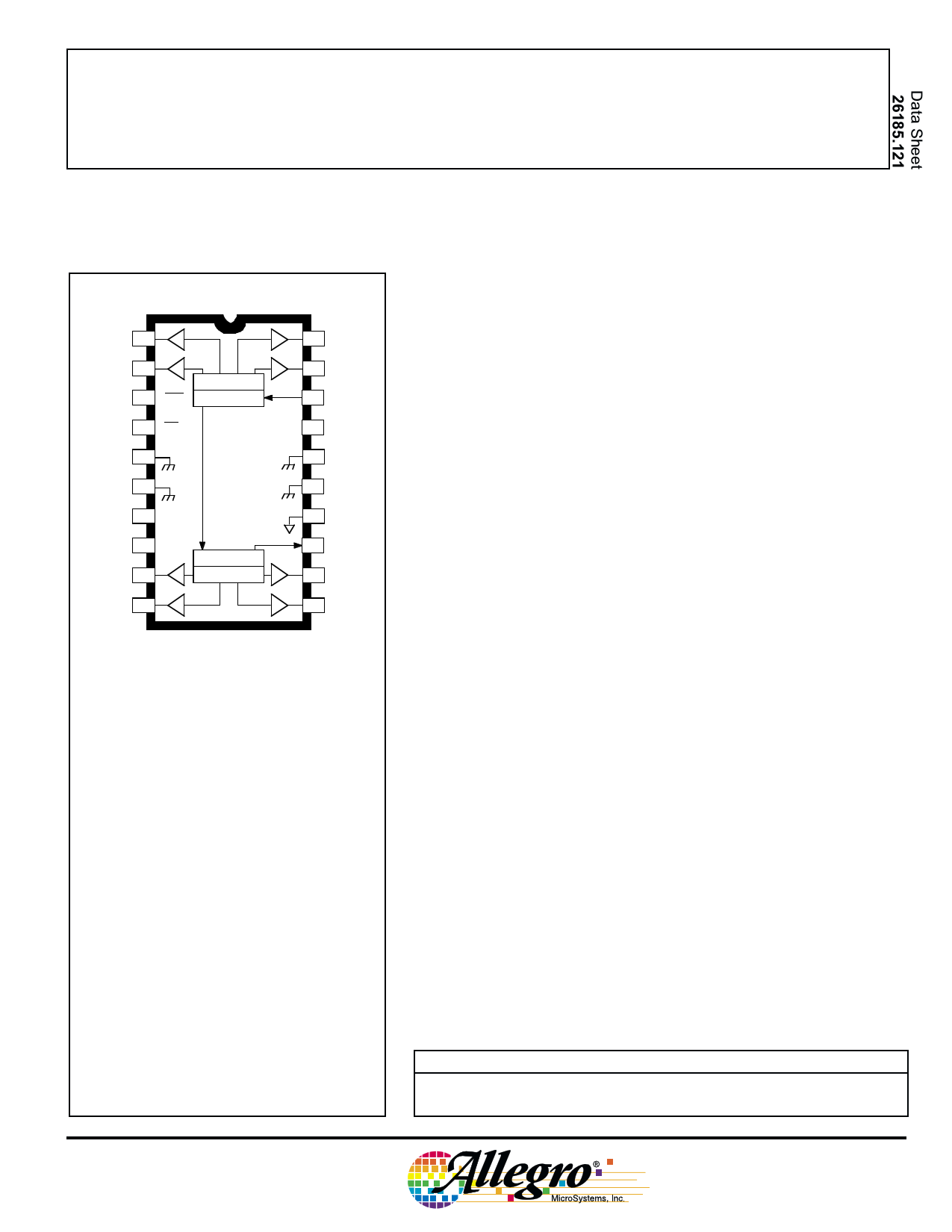
LOGIC SYMBOL
OUTPUT
ENABLE
STROBE
REGISTER
CLEAR
CLOCK
SERIAL
DATA IN
G3
C2
SRG8
R
C1
1D
2 OUT0
OUT 1
OUT 2
OUT 3
OUT 4
OUT 5
OUT 6
2 OUT7
SERIAL
DATA OUT
Dwg. FP-043-2
A. Data Active Time Before Clock Pulse
(Data Set-Up Time), tsu(D) .......................................... 20 ns
B. Data Active Time After Clock Pulse
(Data Hold Time), th(D) .............................................. 20 ns
C. Clock Pulse Width, tw(CLK) ............................................. 40 ns
D. Time Between Clock Activation
and Strobe, tsu(ST) ....................................................... 50 ns
E. Strobe Pulse Width, tw(ST) .............................................. 50 ns
F. Output Enable Pulse Width, tw(OE) ................................ 4.5 µs
NOTE – Timing is representative of a 12.5 MHz clock.
Higher speeds are attainable.
Serial data present at the input is transferred to the shift
register on the rising edge of the CLOCK input pulse. On
succeeding CLOCK pulses, the registers shift data information
towards the SERIAL DATA OUTPUT.
Information present at any register is transferred to the
respective latch on the rising edge of the STROBE input pulse
(serial-to-parallel conversion).
When the OUTPUT ENABLE input is high, the output
source drivers are disabled (OFF). The information stored in the
latches is not affected by the OUTPUT ENABLE input. With
the OUTPUT ENABLE input low, the outputs are controlled by
the state of their respective latches.
www.allegromicro.com
5 Page | ||
| Páginas | Total 10 Páginas | |
| PDF Descargar | [ Datasheet 6A595.PDF ] | |
Hoja de datos destacado
| Número de pieza | Descripción | Fabricantes |
| 6A595 | 8-BIT SERIAL-INPUT/ DMOS POWER DRIVER | Allegro MicroSystems |
| Número de pieza | Descripción | Fabricantes |
| SLA6805M | High Voltage 3 phase Motor Driver IC. |
Sanken |
| SDC1742 | 12- and 14-Bit Hybrid Synchro / Resolver-to-Digital Converters. |
Analog Devices |
|
DataSheet.es es una pagina web que funciona como un repositorio de manuales o hoja de datos de muchos de los productos más populares, |
| DataSheet.es | 2020 | Privacy Policy | Contacto | Buscar |