|
|
|
PDF FDD6676 Data sheet ( Hoja de datos )
| Número de pieza | FDD6676 | |
| Descripción | 30V N-Channel PowerTrench MOSFET | |
| Fabricantes | Fairchild Semiconductor | |
| Logotipo | ||
Hay una vista previa y un enlace de descarga de FDD6676 (archivo pdf) en la parte inferior de esta página. Total 6 Páginas | ||
|
No Preview Available !
April 2001
FDD6676
30V N-Channel PowerTrench MOSFET
General Description
This N-Channel MOSFET has been designed
specifically to improve the overall efficiency of DC/DC
converters using either synchronous or conventional
switching PWM controllers. It has been optimized for
low gate charge, low RDS( ON) and fast switching speed.
extremely low RDS(ON) in a small package.
Applications
• DC/DC converter
• Motor Drives
Features
• 78 A, 30 V
RDS(ON) = 7.5 mΩ @ VGS = 10 V
RDS(ON) = 8.5 mΩ @ VGS = 4.5 V
• Low gate charge
• Fast Switching
• High performance trench technology for extremely
low RDS(ON)
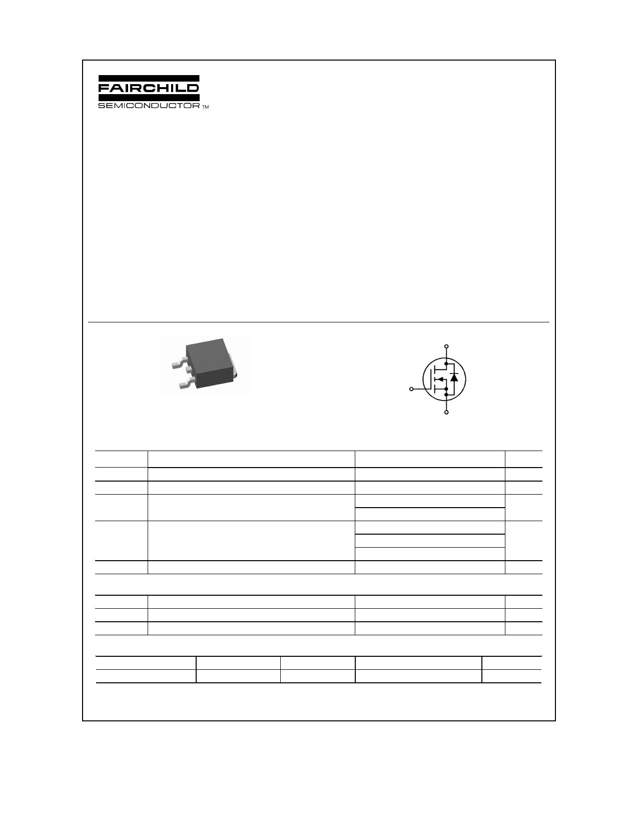
D
G
S
TO-252
Absolute Maximum Ratings TA=25oC unless otherwise noted
Symbol
VDSS
VGSS
ID
PD
Parameter
Drain-Source Voltage
Gate-Source Voltage
Drain Current – Continuous
– Pulsed
Power Dissipation for Single Operation
(Note 3)
(Note 1a)
(Note 1)
(Note 1a)
(Note 1b)
TJ, TSTG
Operating and Storage Junction Temperature Range
Thermal Characteristics
RθJC Thermal Resistance, Junction-to-Case
RθJA Thermal Resistance, Junction-to-Ambient
RθJA Thermal Resistance, Junction-to-Ambient
(Note 1)
(Note 1a)
(Note 1b)
Package Marking and Ordering Information
Device Marking
Device
Reel Size
FDD6676
FDD6676
13’’
D
G
S
Ratings
30
±16
78
100
83
3.8
1.6
-55 to +175
1.8
40
96
Tape width
12mm
Units
V
V
A
W
°C
°C/W
°C/W
°C/W
Quantity
2500 units
2001 Fairchild Semiconductor Corporation
FDD6676 Rev C(W)
1 page 
Typical Characteristics
10
ID = 16.8A
8
6
VDS = 5.0V
15V
10V
4
2
0
0 10 20 30 40 50 60 70 80 90
Qg, GATE CHARGE (nC)
Figure 7. Gate Charge Characteristics
1000
100
RDS(ON) LIMIT
10
1
VGS = 10V
SINGLE PULSE
0.1 RθJA = 96oC/W
TA = 25oC
100µs
1ms
10ms
100ms
1s
10s
DC
0.01
0.1
1 10
VDS, DRAIN-SOURCE VOLTAGE (V)
100
Figure 9. Maximum Safe Operating Area
7000
6000
5000
4000
3000
2000
1000
0
0
CISS
f = 1 MHz
VGS = 0 V
COSS
CRSS
5 10 15 20 25
VDS, DRAIN TO SOURCE VOLTAGE (V)
30
Figure 8. Capacitance Characteristics
50
SINGLE PULSE
40 RθJA = 96°C/W
TA = 25°C
30
20
10
0
0.001
0.01
0.1 1
t1, TIME (sec)
10 100
Figure 10. Single Pulse Maximum
Power Dissipation
1
0.1
0.01
D = 0.5
0.2
0.1
0.05
0.02
0.01
SINGLE PULSE
0.001
0.0001
0.001
0.01
0.1 1
t1, TIME (sec)
RθJA(t) = r(t) + RθJA
RθJA = 96oC/W
P(pk)
t1
t2
TJ - TA = P * RθJA(t)
Duty Cycle, D = t1 / t2
10 100 1000
Figure 11. Transient Thermal Response Curve
Thermal characterization performed using the conditions described in Note 1b.
Transient thermal response will change depending on the circuit board design.
FDD6676 Rev. C(W)
5 Page | ||
| Páginas | Total 6 Páginas | |
| PDF Descargar | [ Datasheet FDD6676.PDF ] | |
Hoja de datos destacado
| Número de pieza | Descripción | Fabricantes |
| FDD6670 | N-Channel/ Logic Level/ PowerTrench MOSFET | Fairchild Semiconductor |
| FDD6670A | N-Channel/ Logic Level/ PowerTrench MOSFET | Fairchild Semiconductor |
| FDD6670AL | 30V N-Channel PowerTrench MOSFET | Fairchild Semiconductor |
| FDD6670S | 30V N-Channel PowerTrench SyncFET | Fairchild Semiconductor |
| Número de pieza | Descripción | Fabricantes |
| SLA6805M | High Voltage 3 phase Motor Driver IC. |
Sanken |
| SDC1742 | 12- and 14-Bit Hybrid Synchro / Resolver-to-Digital Converters. |
Analog Devices |
|
DataSheet.es es una pagina web que funciona como un repositorio de manuales o hoja de datos de muchos de los productos más populares, |
| DataSheet.es | 2020 | Privacy Policy | Contacto | Buscar |