|
|
|
PDF 4066 Data sheet ( Hoja de datos )
| Número de pieza | 4066 | |
| Descripción | Quad Analog Switch/Quad Multiplexer | |
| Fabricantes | ON Semiconductor | |
| Logotipo | ||
Hay una vista previa y un enlace de descarga de 4066 (archivo pdf) en la parte inferior de esta página. Total 12 Páginas | ||
|
No Preview Available !
MC14066B
Quad Analog Switch/Quad
Multiplexer
The MC14066B consists of four independent switches capable of
controlling either digital or analog signals. This quad bilateral switch
is useful in signal gating, chopper, modulator, demodulator and
CMOS logic implementation.
The MC14066B is designed to be pin–for–pin compatible with the
MC14016B, but has much lower ON resistance. Input voltage swings
as large as the full supply voltage can be controlled via each
independent control input.
• Triple Diode Protection on All Control Inputs
• Supply Voltage Range = 3.0 Vdc to 18 Vdc
• Linearized Transfer Characteristics
• Low Noise — 12 nV/√Cycle, f ≥ 1.0 kHz typical
• Pin–for–Pin Replacement for CD4016, CD4016, MC14016B
• For Lower RON, Use The HC4066 High–Speed CMOS Device
MAXIMUM RATINGS (Voltages Referenced to VSS) (Note 2.)
Symbol
Parameter
Value
Unit
VDD
Vin, Vout
DC Supply Voltage Range
Input or Output Voltage Range
(DC or Transient)
– 0.5 to +18.0
– 0.5 to VDD + 0.5
V
V
Iin Input Current (DC or Transient)
per Control Pin
± 10
mA
ISW Switch Through Current
PD Power Dissipation,
per Package (Note 3.)
± 25 mA
500 mW
TA Ambient Temperature Range
Tstg Storage Temperature Range
TL Lead Temperature
(8–Second Soldering)
– 55 to +125
– 65 to +150
260
°C
°C
°C
2. Maximum Ratings are those values beyond which damage to the device
may occur.
3. Temperature Derating:
Plastic “P and D/DW” Packages: – 7.0 mW/_C From 65_C To 125_C
This device contains protection circuitry to guard against damage due to high
static voltages or electric fields. However, precautions must be taken to avoid
applications of any voltage higher than maximum rated voltages to this
v vhigh–impedance circuit. For proper operation, Vin and Vout should be constrained
to the range VSS (Vin or Vout) VDD.
Unused inputs must always be tied to an appropriate logic voltage level (e.g.,
either VSS or VDD). Unused outputs must be left open.
© Semiconductor Components Industries, LLC, 2000
March, 2000 – Rev. 3
1
http://onsemi.com
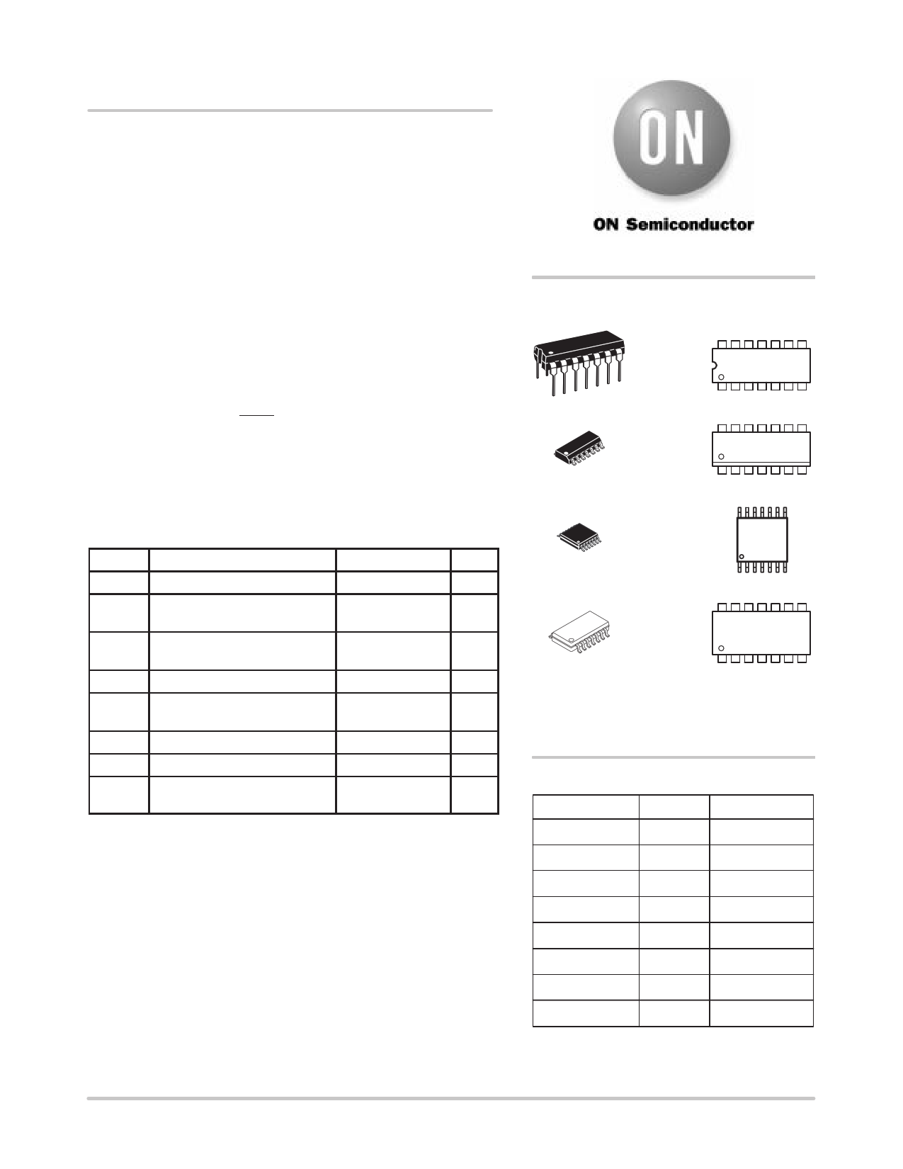
PDIP–14
P SUFFIX
CASE 646
SOIC–14
D SUFFIX
CASE 751A
TSSOP–14
DT SUFFIX
CASE 948G
MARKING
DIAGRAMS
14
MC14066BCP
AWLYYWW
1
14
14066B
AWLYWW
1
14
14
066B
ALYW
SOEIAJ–14
F SUFFIX
CASE 965
1
14
MC14066B
AWLYWW
1
A = Assembly Location
WL or L = Wafer Lot
YY or Y = Year
WW or W = Work Week
ORDERING INFORMATION
Device
Package
Shipping
MC14066BCP
PDIP–14
2000/Box
MC14066BD
SOIC–14
55/Rail
MC14066BDR2 SOIC–14 2500/Tape & Reel
MC14066BDT
TSSOP–14
96/Rail
MC14066BDTEL TSSOP–14 2000/Tape & Reel
MC14066BDTR2 TSSOP–14 2500/Tape & Reel
MC14066BF
SOEIAJ–14 See Note 1.
MC14066BFEL SOEIAJ–14 See Note 1.
1. For ordering information on the EIAJ version of
the SOIC packages, please contact your local
ON Semiconductor representative.
Publication Order Number:
MC14066B/D
1 page 
MC14066B
TEST CIRCUITS
CONTROL
SECTION
OF IC
SOURCE
ON SWITCH
LOAD
V
VC
VC
Vout
Vout
20 ns
tPZH
10%
tPZL
90%
Vout
RL CL
Vin Vx
90% VDD
50%
10% tPHZVSS
90%
Vin = VDD
tPLZ Vx = VSS
Vin = VSS
10% Vx = VDD
Figure 1. ∆V Across Switch
Figure 2. Turn–On Delay Time Test Circuit
and Waveforms
VC = VDD FOR BANDWIDTH TEST
VC = VSS FOR FEEDTHROUGH TEST
VDD – VSS
2
Vin Vout
RL CL
VC
VDD VSS
Figure 3. Bandwidth and
Feedthrough Attenuation
VDD – VSS
2
Vin
VDD
RL CL
VSS RL
Figure 4. Channel Separation
CL
Vin
1k
RL
10 k
VC = – 5.0 V TO + 5.0 V SWING
Figure 5. Crosstalk,
Control to Output
Vout
CL = 50 pF
CONTROL
SECTION
OF IC
OFF CHANNEL UNDER TEST
VDD
A VSS
VSS
VDD
Figure 6. Off Channel Leakage
http://onsemi.com
5
5 Page 
14
1
e
Z
D
b
0.13 (0.005) M
MC14066B
PACKAGE DIMENSIONS
F SUFFIX
PLASTIC EIAJ SOIC PACKAGE
CASE 965–01
ISSUE O
8
E HE
7
LE
M_
Q1
L
DETAIL P
VIEW P
A
c
A1
0.10 (0.004)
NOTES:
1. DIMENSIONING AND TOLERANCING PER ANSI
Y14.5M, 1982.
2. CONTROLLING DIMENSION: MILLIMETER.
3. DIMENSIONS D AND E DO NOT INCLUDE
MOLD FLASH OR PROTRUSIONS AND ARE
MEASURED AT THE PARTING LINE. MOLD FLASH
OR PROTRUSIONS SHALL NOT EXCEED 0.15
(0.006) PER SIDE.
4. TERMINAL NUMBERS ARE SHOWN FOR
REFERENCE ONLY.
5. THE LEAD WIDTH DIMENSION (b) DOES NOT
INCLUDE DAMBAR PROTRUSION. ALLOWABLE
DAMBAR PROTRUSION SHALL BE 0.08 (0.003)
TOTAL IN EXCESS OF THE LEAD WIDTH
DIMENSION AT MAXIMUM MATERIAL CONDITION.
DAMBAR CANNOT BE LOCATED ON THE LOWER
RADIUS OR THE FOOT. MINIMUM SPACE
BETWEEN PROTRUSIONS AND ADJACENT LEAD
TO BE 0.46 ( 0.018).
MILLIMETERS
INCHES
DIM MIN MAX MIN MAX
A ––– 2.05 ––– 0.081
A1 0.05 0.20 0.002 0.008
b 0.35 0.50 0.014 0.020
c 0.18 0.27 0.007 0.011
D 9.90 10.50 0.390 0.413
E 5.10 5.45 0.201 0.215
e 1.27 BSC
0.050 BSC
HE 7.40 8.20 0.291 0.323
0.50 0.50 0.85 0.020 0.033
LE 1.10 1.50 0.043 0.059
M 0 _ 10 _ 0 _ 10 _
Q1 0.70 0.90 0.028 0.035
Z ––– 1.42 ––– 0.056
http://onsemi.com
11
11 Page | ||
| Páginas | Total 12 Páginas | |
| PDF Descargar | [ Datasheet 4066.PDF ] | |
Hoja de datos destacado
| Número de pieza | Descripción | Fabricantes |
| 4060AL | N-Channel Enhancement Mode Field Effect Transistor | Chino-Excel Technology |
| 4060R | Radial Lead Resistor | International Resistive |
| 4066 | Quad Bilateral Switch | National Semiconductor |
| 4066 | Quad Analog Switch/Quad Multiplexer | ON Semiconductor |
| Número de pieza | Descripción | Fabricantes |
| SLA6805M | High Voltage 3 phase Motor Driver IC. |
Sanken |
| SDC1742 | 12- and 14-Bit Hybrid Synchro / Resolver-to-Digital Converters. |
Analog Devices |
|
DataSheet.es es una pagina web que funciona como un repositorio de manuales o hoja de datos de muchos de los productos más populares, |
| DataSheet.es | 2020 | Privacy Policy | Contacto | Buscar |