|
|
|
PDF LTC1871 Data sheet ( Hoja de datos )
| Número de pieza | LTC1871 | |
| Descripción | Wide Input Range/ No RSENSE Current Mode Boost/ Flyback and SEPIC Controller | |
| Fabricantes | Linear Technology | |
| Logotipo | ||
Hay una vista previa y un enlace de descarga de LTC1871 (archivo pdf) en la parte inferior de esta página. Total 36 Páginas | ||
|
No Preview Available !
LTC1871
Wide Input Range, No RSENSETM
Current Mode Boost, Flyback and SEPIC Controller
FEATURES
s High Efficiency (No Sense Resistor Required)
s Wide Input Voltage Range: 2.5V to 36V
s Current Mode Control Provides Excellent
Transient Response
s High Maximum Duty Cycle (92% Typ)
s ±2% RUN Pin Threshold with 100mV Hysteresis
s ±1% Internal Voltage Reference
s Micropower Shutdown: IQ = 10µA
s Programmable Operating Frequency
(50kHz to 1MHz) with One External Resistor
s Synchronizable to an External Clock Up to 1.3 × fOSC
s User-Controlled Pulse Skip or Burst Mode® Operation
s Internal 5.2V Low Dropout Voltage Regulator
s Output Overvoltage Protection
s Capable of Operating with a Sense Resistor for High
Output Voltage Applications
s Small 10-Lead MSOP Package
U
APPLICATIO S
s Telecom Power Supplies
s Portable Electronic Equipment
DESCRIPTIO
The LTC®1871 is a wide input range, current mode, boost,
flyback and SEPIC controller that drives an N-channel
power MOSFET and requires very few external compo-
nents. Intended for low to medium power applications, it
eliminates the need for a current sense resistor by utiliz-
ing the power MOSFET’s on-resistance, thereby maximiz-
ing efficiency.
The IC’s operating frequency can be set with an external
resistor over a 50kHz to 1MHz range, and can be synchro-
nized to an external clock using the MODE/SYNC pin.
Burst Mode operation at light loads, a low minimum
operating supply voltage of 2.5V and a low shutdown
quiescent current of 10µA make the LTC1871 ideally
suited for battery-operated systems.
For applications requiring constant frequency operation,
Burst Mode operation can be defeated using the MODE/
SYNC pin. Higher output voltage boost, SEPIC and fly-
back applications are possible with the LTC1871 by
connecting the SENSE pin to a resistor in the source of the
power MOSFET.
The LTC1871 is available in the 10-lead MSOP package.
, LTC and LT are registered trademarks of Linear Technology Corporation.
Burst Mode is a registered trademark of Linear Technology Corporation.
No RSENSE is a trademark of Linear Technology Corporation.
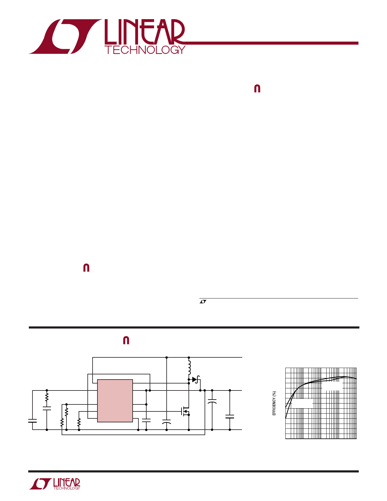
TYPICAL APPLICATIO
L1
1µH
D1
VIN
3.3V
RC
22k
CC1
6.8nF
CC2
47pF
R2
37.4k
1%
R1
12.1k
1%
RT
80.6k
1%
RUN SENSE
ITH VIN
LTC1871
FB
FREQ
INTVCC
GATE
MODE/SYNC GND
CVCC +
4.7µF
X5R
CIN
22µF
6.3V
×2
M1
CIN: TAIYO YUDEN JMK325BJ226MM
COUT1: PANASONIC EEFUEOJ151R
COUT2: TAIYO YUDEN JMK325BJ226MM
D1: MBRB2515L
L1: SUMIDA CEP125-H 1R0MH
M1: FAIRCHILD FDS7760A
VOUT
5V
+ COUT1
150µF
7A
(10A PEAK)
6.3V
×4 COUT2
22µF
6.3V
X5R
×2
GND
1871 F01a
Figure 1. High Efficiency 3.3V Input, 5V Output Boost Converter (Bootstrapped)
Efficiency of Figure 1
100
90
Burst Mode
80 OPERATION
70
PULSE-SKIP
60 MODE
50
40
30
0.001
0.01 0.1
1
OUTPUT CURRENT (A)
10
1871 F01b
1
1 page 
TYPICAL PERFOR A CE CHARACTERISTICS
RUN Thresholds vs VIN
1.5
RUN Thresholds vs Temperature
1.40
LTC1871
RT vs Frequency
1000
1.35
1.4
1.30
1.3
1.25
100
1.2
0
10 20 30
VIN (V)
40
1871 G10
Frequency vs Temperature
325
320
315
310
305
300
295
290
285
280
275
–50 –25 0 25 50 75 100 125 150
TEMPERATURE (°C)
1871 G13
INTVCC Load Regulation
VIN = 7.5V
5.2
5.1
5.0
0
10 20 30 40 50 60 70 80
INTVCC LOAD (mA)
1871 G16
1.20
–50 –25
0 25 50 75 100 125 150
TEMPERATURE (°C)
1871 G11
Maximum Sense Threshold
vs Temperature
160
155
150
145
140
–50 –25 0 25 50 75 100 125 150
TEMPERATURE (°C)
1871 G14
INTVCC Line Regulation
5.4
5.3
5.2
5.1
0
5 10 15 20 25 30 35 40
VIN (V)
1871 G17
10
0 100 200 300 400 500 600 700 800 900 1000
FREQUENCY (kHz)
1871 G12
SENSE Pin Current vs Temperature
35
GATE HIGH
VSENSE = 0V
30
25
–50 –25 0 25 50 75 100 125 150
TEMPERATURE (°C)
INTVCC Dropout Voltage
vs Current, Temperature
500
1871 G15
450
150°C
400
125°C
350
75°C
300
25°C
250
200
0°C
150
–50°C
100
50
0
0 5 10 15 20
INTVCC LOAD (mA)
1871 G18
5
5 Page 
APPLICATIO S I FOR ATIO
1.230V
R2
–
+
LOGIC
VIN
P-CH
R1 5.2V INTVCC
DRIVER
GATE
INPUT
SUPPLY
2.5V TO 30V
CIN
+
CVCC
4.7µF
M1
LTC1871
GND
1871 F07
GND
PLACE AS CLOSE AS
POSSIBLE TO DEVICE PINS
Figure 7. Bypassing the LDO Regulator and Gate Driver Supply
As a result, high input voltage applications in which a large
power MOSFET is being driven at high frequencies can
cause the LTC1871 to exceed its maximum junction
temperature rating. The junction temperature can be
estimated using the following equations:
IQ(TOT) ≈ IQ + f • QG
PIC = VIN • (IQ + f • QG)
TJ = TA + PIC • RTH(JA)
The total quiescent current IQ(TOT) consists of the static
supply current (IQ) and the current required to charge and
discharge the gate of the power MOSFET. The 10-pin
MSOP package has a thermal resistance of RTH(JA) =
120°C/W.
As an example, consider a power supply with VIN = 5V and
VO = 12V at IO = 1A. The switching frequency is 500kHz,
and the maximum ambient temperature is 70°C. The
power MOSFET chosen is the IRF7805, which has a
maximum RDS(ON) of 11mΩ (at room temperature) and a
maximum total gate charge of 37nC (the temperature
coefficient of the gate charge is low).
IQ(TOT) = 600µA + 37nC • 500kHz = 19.1mA
PIC = 5V • 19.1mA = 95mW
TJ = 70°C + 120°C/W • 95mW = 81.4°C
This demonstrates how significant the gate charge current
can be when compared to the static quiescent current in
the IC.
To prevent the maximum junction temperature from being
exceeded, the input supply current must be checked when
operating in a continuous mode at high VIN. A tradeoff
between the operating frequency and the size of the power
MOSFET may need to be made in order to maintain a
reliable IC junction temperature. Prior to lowering the
operating frequency, however, be sure to check with
power MOSFET manufacturers for their latest-and-great-
est low QG, low RDS(ON) devices. Power MOSFET manu-
facturing technologies are continually improving, with
newer and better performance devices being introduced
almost yearly.
Output Voltage Programming
The output voltage is set by a resistor divider according to
the following formula:
VO = 1.230V • 1+ RR21
The external resistor divider is connected to the output as
shown in Figure 1, allowing remote voltage sensing. The
resistors R1 and R2 are typically chosen so that the error
11
11 Page | ||
| Páginas | Total 36 Páginas | |
| PDF Descargar | [ Datasheet LTC1871.PDF ] | |
Hoja de datos destacado
| Número de pieza | Descripción | Fabricantes |
| LTC1871 | Wide Input Range/ No RSENSE Current Mode Boost/ Flyback and SEPIC Controller | Linear Technology |
| LTC1871EMS | Wide Input Range/ No RSENSE Current Mode Boost/ Flyback and SEPIC Controller | Linear Technology |
| LTC1872 | Constant Frequency Current Mode Step-Up DC/DC Controller in SOT-23 | Linear Technology |
| LTC1872ES6 | Constant Frequency Current Mode Step-Up DC/DC Controller in SOT-23 | Linear Technology |
| Número de pieza | Descripción | Fabricantes |
| SLA6805M | High Voltage 3 phase Motor Driver IC. |
Sanken |
| SDC1742 | 12- and 14-Bit Hybrid Synchro / Resolver-to-Digital Converters. |
Analog Devices |
|
DataSheet.es es una pagina web que funciona como un repositorio de manuales o hoja de datos de muchos de los productos más populares, |
| DataSheet.es | 2020 | Privacy Policy | Contacto | Buscar |