|
|
|
PDF HPC26083 Data sheet ( Hoja de datos )
| Número de pieza | HPC26083 | |
| Descripción | High-Performance microControllers | |
| Fabricantes | National Semiconductor | |
| Logotipo | ||
Hay una vista previa y un enlace de descarga de HPC26083 (archivo pdf) en la parte inferior de esta página. Total 36 Páginas | ||
|
No Preview Available !
PRELIMINARY
April 1994
HPC16083 HPC26083 HPC36083 HPC46083
HPC16003 HPC26003 HPC36003 HPC46003
High-Performance microControllers
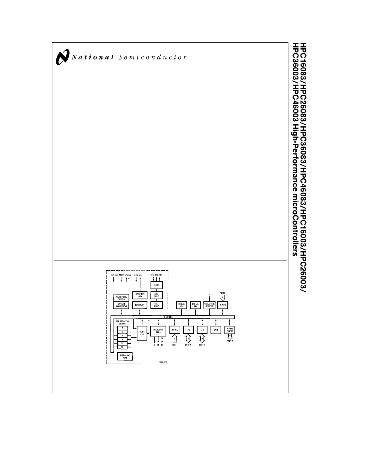
General Description
The HPC16083 and HPC16003 are members of the HPCTM
family of High Performance microControllers Each member
of the family has the same core CPU with a unique memory
and I O configuration to suit specific applications The
HPC16083 has 8k bytes of on-chip ROM The HPC16003
has no on-chip ROM and is intended for use with external
direct memory Each part is fabricated in National’s ad-
vanced microCMOS technology This process combined
with an advanced architecture provides fast flexible I O
control efficient data manipulation and high speed compu-
tation
The HPC devices are complete microcomputers on a single
chip All system timing internal logic ROM RAM and I O
are provided on the chip to produce a cost effective solution
for high performance applications On-chip functions such
as UART up to eight 16-bit timers with 4 input capture regis-
ters vectored interrupts WATCHDOGTM logic and MICRO-
WIRE PLUSTM provide a high level of system integration
The ability to address up to 64k bytes of external memory
enables the HPC to be used in powerful applications typical-
ly performed by microprocessors and expensive peripheral
chips The term ‘‘HPC16083’’ is used throughout this data-
sheet to refer to the HPC16083 and HPC16003 devices un-
less otherwise specified
The microCMOS process results in very low current drain
and enables the user to select the optimum speed power
product for his system The IDLE and HALT modes provide
further current savings The HPC is available in 68-pin
PLCC LDCC PGA and 80-Pin PQFP packages
Features
Y HPC family core features
16-bit architecture both byte and word
16-bit data bus ALU and registers
64k bytes of external direct memory addressing
FAST 200 ns for fastest instruction when using
20 0 MHz clock 134 ns at 30 MHz
High code efficiency most instructions are single
byte
16 x 16 multiply and 32 x 16 divide
Eight vectored interrupt sources
Four 16-bit timer counters with 4 synchronous out-
puts and WATCHDOG logic
MICROWIRE PLUS serial I O interface
CMOS very low power with two power save modes
IDLE and HALT
Y UART full duplex programmable baud rate
Y Four additional 16-bit timer counters with pulse width
modulated outputs
Y Four input capture registers
Y 52 general purpose I O lines (memory mapped)
Y 8k bytes of ROM 256 bytes of RAM on chip
Y ROMless version available (HPC16003)
Y Commercial (0 C to a70 C) industrial (b40 C to
a85 C) automotive (b40 C to a105 C) and military
(b55 C to a125 C) temperature ranges
For applications requiring more RAM and ROM see
HPC16064 data sheet
Block Diagram (HPC16083 with 8k ROM shown)
Series 32000 TapePak and TRI-STATE are registered trademarks of National Semiconductor Corporation
MOLETM HPCTM COPSTM MICROWIRE PLUSTM and WATCHDOGTM are trademarks of National Semiconductor Corporation
UNIX is a registered trademarks of AT T Bell Laboratories
VAXTM is a trademark of Digital Equipment Corporation
IBM and PC AT are registered trademarks of International Business Machines Corporation
SUN is a registered trademark of Sun Microsystems
SunOSTM is a trademark of Sun Microsystems
C1995 National Semiconductor Corporation TL DD 8801
TL DD 8801 – 1
RRD-B30M105 Printed in U S A
1 page 
30 MHz
AC Electrical Characteristics (Continued)
(See Notes 1 and 4 and Figure 1 thru Figure 5 ) VCC e 5 0V g10% unless otherwise specified TA e 0 C to a70 C for
HPC46083 HPC46003 b40 C to a85 C for HPC36083 HPC36003 b40 C to a105 C for HPC26083 HPC26003 b55 C to
a125 C for HPC16083 HPC16003
Symbol and Formula
fC
tC1 e 1 fC
tCKIH
tCKIL
tC e 2 fC
tWAIT e tC
tDC1C2R
tDC1C2F
fU e fC 8
fMW
Parameter
CKI Operating Frequency
CKI Clock Period
CKI High Time
CKI Low Time
CPU Timing Cycle
CPU Wait Sate Period
Delay of CK2 Rising Edge after
CKI Falling Edge
Delay of CK2 Falling Edge after
CKI Falling Edge
External UART Clock Input Frequency
External MICROWIRE PLUS
Clock Input Frequency
Min
2
33
15
16 6
66
66
0
0
Max
30
500
55
55
3 75
1 875
Units
MHz
ns
ns
ns
ns
ns
ns
ns
MHz
MHz
Note
(Note 2)
(Note 2)
fXIN e fC 22
tXIN e tC
External Timer Input Frequency
Pulse Width for Timer Inputs
1 364
MHz
66 ns
tUWS
MICROWIRE Setup Time Master
Slave
100
20
ns
tUWH
MICROWIRE Hold Time Master
Slave
20
50
ns
tUWV
MICROWIRE Output Valid Time Master
Slave
50 ns
150
tSALE e tC a 40
tHWP e tC a 10
tHAE e tC a 85
tHAD e tC a 85
tBF e tC a 66
tBE e tCa 66
tUAS
tUAH
tRPW
tOE
tOD
HLD Falling Edge before ALE Rising Edge
HLD Pulse Width
HLDA Falling Edge after HLD Falling Edge
HLDA Rising Edge after HLD Rising Edge
Bus Float after HLDA Falling Edge
Bus Enable after HLDA Rising Edge
Address Setup Time to Falling Edge of URD
Address Hold Time from Rising Edge of URD
URD Pulse Width
URD Falling Edge to Output Data Valid
Rising Edge of URD to
Output Data Invalid
90
76
99
10
10
100
0
5
151
135
99
60
35
ns
ns
ns (Note 3)
ns
ns (Note 5)
ns (Note 5)
ns
ns
ns
ns
ns (Note 6)
tDRDY
tWDW
tUDS
tUDH
tA
RDRDY Delay from Rising Edge of URD
UWR Pulse Width
Input Data Valid before Rising Edge of UWR
Input Data Hold after Rising Edge of UWR
WRRDY Delay from Rising Edge of UWR
40
10
15
70
70
ns
ns
ns
ns
ns
This maximum frequency is attainable provided that this external baud clock has a duty cycle such that the high period includes two (2) falling edges of the CK2
clock
5
5 Page 
AC Electrical Specifications Test Conditions VCC e 4 5V and 5 5V (Unless Otherwise Specified) (Note 1)
(Continued)
Symbol
Parameter
SBGRP 9
Conditions a25 C
Min Max
SBGRP 10
a125 C
Min Max
tRWP e tC
tSALE e tC a 40
RDY Pulse Width
Falling Edge of HLD to
to Rising Edge of ALE
100 100
115 115
tHWP e tC a 10
tHAD e tC a85
HLD Pulse Width
Rising Edge on HLD to
Rising Edge on HLDA
110 110
160 160
tHAE e tC a100
Falling Edge on HLD to
Falling Edge on HLDA
200 200
tBF e tC a66
BUS Float before
Falling Edge on HLDA
116 116
tBE e tC a66
BUS Enable from
Rising Edge of HLDA
116 116
tUAS
Address Setup Time to
Falling Edge of URD
10 10
tUAH
Address Hold Time from
Rising Edge of URD
10 10
tRPW
tOE
URD Pulse Width
URD Falling Edge to
Data Out Valid
100 100
60 60
tRDRDY
RDY Delay from
Rising Edge of URD
70 70
tWDW
tUDS
UWR Pulse Width
Data Invalid before
Trailing Edge of UWR
40 40
10 10
tUDH
Data In Hold after
Rising Edge of UWR
15 15
tA WRRDY Delay from
Rising Edge of UWR
70 70
Note 1 Electrical end point testing (when required) for groups C D shall consist only of subgroups 1 2 9 and 10
Note 5 Tested in functional patterns Not directly measured
Note 6 CL e 70 pF Input and output levels are per DC characteristics
SBGRP 11
b55 C
Min Max
100
115
110
160
200
116
116
10
10
100
60
70
40
10
15
70
Units Notes
ns (Note 6)
ns (Note 6)
ns (Note 6)
ns (Note 6)
ns (Note 6)
ns (Note 6)
ns (Note 6)
ns (Note 6)
ns (Note 6)
ns (Note 6)
ns (Note 6)
ns (Note 6)
ns (Note 6)
ns (Note 6)
ns (Note 6)
ns (Note 6)
Pin Descriptions
The HPC16083 is available in 68-pin PLCC LDCC PGA
and 80-pin PQFP packages
I O PORTS
Port A is a 16-bit bidirectional I O port with a data direction
register to enable each separate pin to be individually de-
fined as an input or output When accessing external memo-
ry port A is used as the multiplexed address data bus
Port B is a 16-bit port with 12 bits of bidirectional I O similar
in structure to Port A Pins B10 B11 B12 and B15 are gen-
eral purpose outputs only in this mode Port B may also be
configured via a 16-bit function register BFUN to individually
allow each pin to have an alternate function
B0 TDX
UART Data Output
B1
B2 CKX UART Clock (Input or Output)
B3 T2IO Timer2 I O Pin
B4 T3IO Timer3 I O Pin
B5 SO
MICROWIRE PLUS Output
B6 SK
MICROWIRE PLUS Clock (Input or Output)
B7 HLDA Hold Acknowledge Output
B8 TS0
Timer Synchronous Output
B9 TS1
Timer Synchronous Output
B10 UA0
Address 0 Input for UPI Mode
B11 WRRDY Write Ready Output for UPI Mode
B12
B13 TS2
Timer Synchronous Output
11
11 Page | ||
| Páginas | Total 36 Páginas | |
| PDF Descargar | [ Datasheet HPC26083.PDF ] | |
Hoja de datos destacado
| Número de pieza | Descripción | Fabricantes |
| HPC26083 | High-Performance microControllers | National Semiconductor |
| HPC26083 | (HPC16003 - HPC46003 / HPC16083 - HPC46083) High-Performance microControllers | National Semiconductor |
| Número de pieza | Descripción | Fabricantes |
| SLA6805M | High Voltage 3 phase Motor Driver IC. |
Sanken |
| SDC1742 | 12- and 14-Bit Hybrid Synchro / Resolver-to-Digital Converters. |
Analog Devices |
|
DataSheet.es es una pagina web que funciona como un repositorio de manuales o hoja de datos de muchos de los productos más populares, |
| DataSheet.es | 2020 | Privacy Policy | Contacto | Buscar |