|
|
|
PDF AD549 Data sheet ( Hoja de datos )
| Número de pieza | AD549 | |
| Descripción | Ultralow Input Bias Current Operational Amplifier | |
| Fabricantes | Analog Devices | |
| Logotipo | ||
Hay una vista previa y un enlace de descarga de AD549 (archivo pdf) en la parte inferior de esta página. Total 12 Páginas | ||
|
No Preview Available !
a
FEATURES
Ultralow Bias Current: 60 fA max (AD549L)
250 fA max (AD549J)
Input Bias Current Guaranteed Over Common-Mode
Voltage Range
Low Offset Voltage: 0.25 mV max (AD549K)
1.00 mV max (AD549J)
Low Offset Drift: 5 V/؇C max (AD549K)
20 V/؇C max (AD549J)
Low Power: 700 A max Supply Current
Low Input Voltage Noise: 4 V p-p 0.1 Hz to 10 Hz
MIL-STD-883B Parts Available
APPLICATIONS
Electrometer Amplifiers
Photodiode Preamp
pH Electrode Buffer
Vacuum lon Gage Measurement
Ultralow Input Bias Current
Operational Amplifier
AD549*
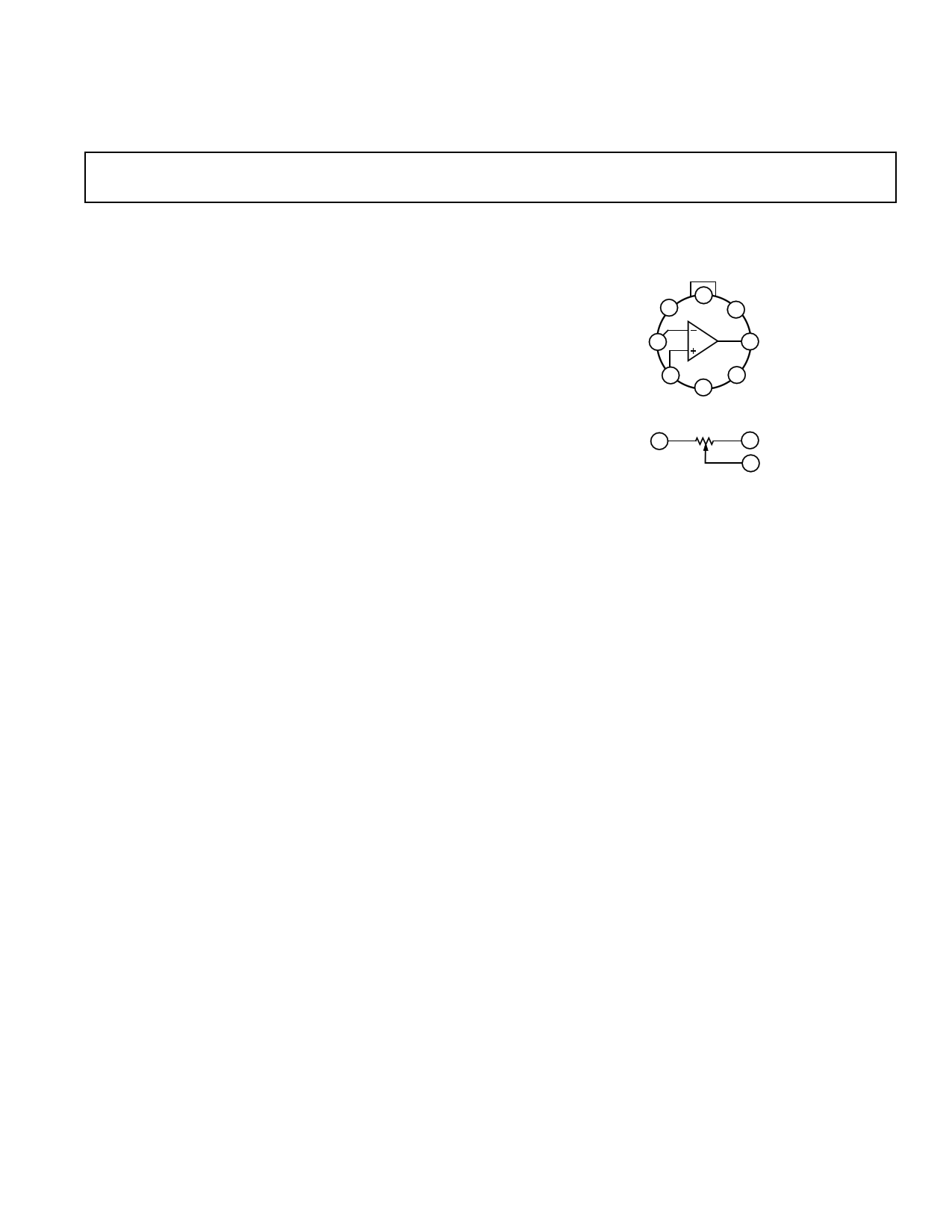
CONNECTION DIAGRAM
GUARD PIN, CONNECTED TO CASE
OFFSET NULL
1
NC
8 V+
AD549 7
INVERTING 2
INPUT
6 OUTPUT
3
NONINVERTING
INPUT
5
4 OFFSET
NULL
V–
10kΩ
1
VOS TRIM
NC = NO CONNECTION
5
4 –15V
PRODUCT DESCRIPTION
The AD549 is a monolithic electrometer operational amplifier
with very low input bias current. Input offset voltage and input
offset voltage drift are laser trimmed for precision performance.
The AD549’s ultralow input current is achieved with “Topgate”
JFET technology, a process development exclusive to Analog
Devices. This technology allows the fabrication of extremely low
input current JFETs compatible with a standard junction-
isolated bipolar process. The 1015 Ω common-mode impedance,
a result of the bootstrapped input stage, insures that the input
current is essentially independent of common-mode voltage.
The AD549 is suited for applications requiring very low input
current and low input offset voltage. It excels as a preamp for a
wide variety of current output transducers such as photodiodes,
photomultiplier tubes, or oxygen sensors. The AD549 can also
be used as a precision integrator or low droop sample and hold.
The AD549 is pin compatible with standard FET and electrom-
eter op amps, allowing designers to upgrade the performance of
present systems at little additional cost.
The AD549 is available in a TO-99 hermetic package. The case
is connected to Pin 8 so that the metal case can be independently
connected to a point at the same potential as the input termi-
nals, minimizing stray leakage to the case.
*Protected by Patent No. 4,639,683.
The AD549 is available in four performance grades. The J, K,
and L versions are rated over the commercial temperature range
0°C to +70°C. The S grade is specified over the military tem-
perature range of –55°C to +125°C and is available processed to
MIL-STD-883B, Rev C. Extended reliability PLUS screening is
also available. Plus screening includes 168-hour burn-in, as
well as other environmental and physical tests derived from
MIL-STD-883B, Rev C.
PRODUCT HIGHLIGHTS
1. The AD549’s input currents are specified, 100% tested and
guaranteed after the device is warmed up. Input current is
guaranteed over the entire common-mode input voltage
range.
2. The AD549’s input offset voltage and drift are laser trimmed
to 0.25 mV and 5 µV/°C (AD549K), 1 mV and 20 µV/°C
(AD549J).
3. A maximum quiescent supply current of 700 µA minimizes
heating effects on input current and offset voltage.
4. AC specifications include 1 MHz unity gain bandwidth and
3 V/µs slew rate. Settling time for a 10 V input step is 5 µs to
0.01%.
5. The AD549 is an improved replacement for the AD515,
OPA104, and 3528.
REV. A
Information furnished by Analog Devices is believed to be accurate and
reliable. However, no responsibility is assumed by Analog Devices for its
use, nor for any infringements of patents or other rights of third parties
which may result from its use. No license is granted by implication or
otherwise under any patent or patent rights of Analog Devices.
One Technology Way, P.O. Box 9106, Norwood, MA 02062-9106, U.S.A.
Tel: 617/329-4700
Fax: 617/326-8703
1 page 
50
45
40
35
30
25
20
0
5 10 15
POWER SUPPLY VOLTAGE ± V
Figure 10. Input Bias Current
vs. Supply Voltage
20
160
140
120
100
80
60
40
20
10
100 1k
FREQUENCY – Hz
10k
Figure 11. Input Voltage Noise
Spectral Density
AD549
100k
10k
WHENEVER JOHNSON NOISE IS GREATER THAN
AMPLIFIER NOISE, AMPLIFIER NOISE CAN BE
CONSIDERED NEGLIGIBLE FOR THE APPLICATION
1kHz BANDWIDTH
RESISTOR
1k JOHNSON NOISE
100
10
10Hz
BANDWIDTH
1 AMPLIFIER GENERATED NOISE
0.1
100k 1M 10M 100M 1G 10G 100G
SOURCE RESISTANCE – Ω
Figure 12. Noise vs. Source
Resistance
100 100
80 80
60 60
40 40
20 20
00
–20 –20
–40
10 100
1k 10k 100k 1M
FREQUENCY – Hz
Figure 13. Open-Loop
Frequency Response
–40
10M
40
35
30
25
20
15
10
5
0
10 100
1k 10k 100k
FREQUENCY – Hz
Figure 14. Large Signal
Frequency Response
1M
100
80
60
40
20
0
–20
10 100
1k 10k 100k 1M
FREQUENCY – Hz
10M
Figure 15. CMRR vs. Frequency
REV. A
120
100
80
+ SUPPLY
60
40
– SUPPLY
20
0
–20
10 100
1k 10k 100k 1M
FREQUENCY – Hz
10M
Figure 16. PSRR vs. Frequency
10
5 10mV
5mV
1mV
0
10mV
5mV
–5
1mV
–10
0
1 2 34
SETTLING TIME – µs
5
Figure 17. Output Voltage
Swing and Error vs.
Settling Time
–5–
5 Page 
Figure 43. Photodiode Preamp Noise Sources
AD549
tracter section’s gain for positive and negative inputs matched
over temperature.
Frequency compensation is provided by R11, R12, and C1 and
C2. The bandwidth of the circuit is 300 kHz at input signals
greater than 50 µA, and decreases smoothly with decreasing
signal levels.
To trim the circuit, set the input currents to 10 µA and trim
A3’s offset using the amplifier’s trim potentiometer so the out-
put equals 0. Then set I1 to 1 µA and adjust the output to equal
1 V by trimming R10. Additional offset trims on the amplifiers
A1 and A2 can be used to increase the voltage input accuracy
and dynamic range.
The very low input current of the AD549 makes this circuit use-
ful over a very wide range of signal currents. The total input
current (which determines the low level accuracy of the circuit)
is the sum of the amplifier input current, the leakage across the
compensating capacitor (negligible if polystyrene or Teflon ca-
pacitor is used), and the collector to collector, and collector to
base leakages of one side of the dual log transistors. The magni-
tude of these last two leakages depend on the amplifier’s input
offset voltage and are typically less than 10 fA with 1 mV offsets.
The low level accuracy is limited primarily by the amplifier’s in-
put current, only 60 fA maximum when the AD549L is used.
Figure 44. Photodiode Preamp Noise Sources’ Spectral
Density vs. Frequency
Log Ratio Amplifier
Logarithmic ratio circuits are useful for processing signals with
wide dynamic range. The AD549L’s 60 fA maximum input cur-
rent makes it possible to build a log ratio amplifier with 1% log
conformance for input current ranging from 10 pA to 1 mA, a
dynamic range of 160 dB.
The log ratio amplifier in Figure 45 provides an output voltage
proportional to the log base 10 of the ratio of the input currents
I1 and I2. Resistors R1 and R2 are provided for voltage inputs.
Since NPN devices are used in the feedback loop of the front-
end amplifiers that provide the log transfer function, the output
is valid only for positive input voltages and input currents. The
input currents set the collector currents IC1 and IC2 of a
matched pair of log transistors Q1 and Q2 to develop voltages
VA and VB:
VA, B = – (kT/q) ln IC/IES
where IES is the transistors’ saturation current.
The difference of VA and VB is taken by the subtractor section
to obtain:
VC = (kT/q) ln (IC2/IC1)
VC is scaled up by the ratio of (R9 + R10)/R8, which is equal to
approximately 16 at room temperature, resulting in the output
voltage:
VOUT = 1 × log (IC2/IC1) V.
R8 is a resistor with a positive 3500 ppm/°C temperature coeffi-
cient to provide the necessary temperature compensation. The
parallel combination of R15 and R7 is provided to keep the sub
Figure 45. Log Ratio Amplifier
The effects of the emitter resistance of Q1 and Q2 can degrade
the circuit’s accuracy at input currents above 100 µA. The net-
works composed of R13, D1, R16, and R14, D2, R17 compen-
sate for these errors, so that this circuit has less than 1% log
conformance error at 1 mA input currents. The correct value
for R13 and R14 depends on the type of log transistors used.
49.9 kΩ resistors were chosen for use with LM394 transistors.
Smaller resistance values will be needed for smaller log
transistors.
REV. A
–11–
11 Page | ||
| Páginas | Total 12 Páginas | |
| PDF Descargar | [ Datasheet AD549.PDF ] | |
Hoja de datos destacado
| Número de pieza | Descripción | Fabricantes |
| AD5405 | Dual 12-Bit/ High Bandwidth/ Multiplying DAC with 4-Quadrant Resistors and Parallel Interface | Analog Devices |
| AD5410 | Current Source DAC | Analog Devices |
| AD5412 | (AD5412 / AD5422) Current Source & Voltage Output DAC | Analog Devices |
| AD5415 | (AD5424 - AD5547) High Bandwidth Multiplying DACs | Analog Devices |
| Número de pieza | Descripción | Fabricantes |
| SLA6805M | High Voltage 3 phase Motor Driver IC. |
Sanken |
| SDC1742 | 12- and 14-Bit Hybrid Synchro / Resolver-to-Digital Converters. |
Analog Devices |
|
DataSheet.es es una pagina web que funciona como un repositorio de manuales o hoja de datos de muchos de los productos más populares, |
| DataSheet.es | 2020 | Privacy Policy | Contacto | Buscar |