No Preview Available !

a
16-Bit, 250 kSPS CMOS ADC
AD7663
FEATURES
Throughput: 250 kSPS
INL: ؎3 LSB Max (؎0.0046% of Full Scale)
16-Bit Resolution with No Missing Codes
S/(N+D): 90 dB Typ @ 100 kHz
THD: –100 dB Typ @ 100 kHz
Analog Input Voltage Ranges
Bipolar: ؎10 V, ؎5 V, ؎2.5 V
Unipolar: 0 V to 10 V, 0 V to 5 V, 0 V to 2.5 V
Both AC and DC Specifications
No Pipeline Delay
Parallel (8/16 Bits) and Serial 5 V/3 V Interface
SPI®/QSPI™/MICROWIRE™/DSP Compatible
Single 5 V Supply Operation
Power Dissipation
35 mW Typical
15 W @ 100 SPS
Power-Down Mode: 7 W Max
Package: 48-Lead Quad Flatpack (LQFP)
Package: 48-Lead Chip Scale (LFCSP)
Pin-to-Pin Compatible with the AD7660/AD7664/AD7665
APPLICATIONS
Data Acquisition
Motor Control
Communication
Instrumentation
Spectrum Analysis
Medical Instruments
Process Control
GENERAL DESCRIPTION
The AD7663 is a 16-bit, 250 kSPS, charge redistribution SAR,
analog-to-digital converter that operates from a single 5 V power
supply. It contains a high speed 16-bit sampling ADC, a resistor
input scaler that allows various input ranges, an internal conver-
sion clock, error correction circuits, and both serial and parallel
system interface ports.
The AD7663 is hardware factory-calibrated and is comprehen-
sively tested to ensure such ac parameters as signal-to-noise ratio
(SNR) and total harmonic distortion (THD), in addition to the
more traditional dc parameters of gain, offset, and linearity.
It is fabricated using Analog Devices’ high performance, 0.6 micron
CMOS process and is available in a 48-lead LQFP and a tiny
48-lead LFCSP with operation specified from –40°C to +85°C.
REV. B
FUNCTIONAL BLOCK DIAGRAM
AVDD AGND REF REFGND
DVDD DGND
IND(4R)
INC(4R)
INB(2R)
INA(R)
INGND
PD
RESET
4R
AD7663
4R
2R
R
SWITCHED
CAP DAC
SERIAL
PORT
CLOCK
PARALLEL 16
INTERFACE
CONTROL LOGIC AND
CALIBRATION CIRCUITRY
CNVST
OVDD
OGND
SER/PAR
BUSY
D[15:0]
CS
RD
OB/2C
BYTESWAP
PulSAR Selection
Type/kSPS
Pseudo
Differential
True Bipolar
True Differential
100–250
AD7660
AD7663
AD7675
500–570
AD7650
AD7664
AD7665
AD7676
18-Bit
Simultaneous/
Multichannel
AD7678
AD7679
AD7654
800–1000
AD7671
AD7677
AD7674
AD7655
PRODUCT HIGHLIGHTS
1. Fast Throughput
The AD7663 is a 250 kSPS charge redistribution, 16-bit
SAR ADC with various bipolar and unipolar input ranges.
2. Single-Supply Operation
The AD7663 operates from a single 5 V supply and dissipates
only 35 mW typical. Its power dissipation decreases with
the throughput to, for instance, only 15 µW at a 100 SPS
throughput.
It consumes 7 µW maximum when in power-down.
3. Superior INL
The AD7663 has a maximum integral nonlinearity of 3 LSB
with no missing 16-bit code.
4. Serial or Parallel Interface
Versatile parallel (8 bits or 16 bits) or 2-wire serial interface
arrangement compatible with both 3 V or 5 V logic.
Information furnished by Analog Devices is believed to be accurate and
reliable. However, no responsibility is assumed by Analog Devices for its
use, nor for any infringements of patents or other rights of third parties that
may result from its use. No license is granted by implication or otherwise
under any patent or patent rights of Analog Devices. Trademarks and
registered trademarks are the property of their respective companies.
One Technology Way, P.O. Box 9106, Norwood, MA 02062-9106, U.S.A.
Tel: 781/329-4700
www.analog.com
Fax: 781/326-8703 © 2003 Analog Devices, Inc. All rights reserved.

AD7663
TIMING SPECIFICATIONS (continued)
Parameter
Symbol Min Typ Max
Refer to Figures 17 and 18 (Master Serial Interface Modes)1
CS HIGH to SYNC HI-Z
CS HIGH to Internal SCLK HI-Z
CS HIGH to SDOUT HI-Z
BUSY HIGH in Master Serial Read after Convert
CNVST LOW to SYNC Asserted Delay
(Master Serial Read after Convert)
SYNC Deasserted to BUSY LOW Delay
t25
t26
t27
t28
t29
t30
See Table II
1.25
10
10
10
25
Refer to Figures 19 and 21 (Slave Serial Interface Modes)
External SCLK Setup Time
External SCLK Active Edge to SDOUT Delay
SDIN Setup Time
SDIN Hold Time
External SCLK Period
External SCLK HIGH
External SCLK LOW
t31
t32
t33
t34
t35
t36
t37
5
3
5
5
25
10
10
16
NOTES
1In serial interface modes, the SYNC, SCLK, and SDOUT timings are defined with a maximum load C L of 10 pF; otherwise, the load is 60 pF maximum.
2In Serial Master Read during Convert Mode. See Table II for Master Read after Convert Mode.
Specifications subject to change without notice.
Unit
ns
ns
ns
µs
µs
ns
ns
ns
ns
ns
ns
ns
ns
Table II. Serial Clock Timings in Master Read after Convert
DIVSCLK[1]
DIVSCLK[0]
SYNC to SCLK First Edge Delay Minimum
Internal SCLK Period Minimum
Internal SCLK Period Maximum
Internal SCLK HIGH Minimum
Internal SCLK LOW Minimum
SDOUT Valid Setup Time Minimum
SDOUT Valid Hold Time Minimum
SCLK Last Edge to SYNC Delay Minimum
BUSY HIGH Width Maximum
t18
t19
t19
t20
t21
t22
t23
t24
t28
001
010
4 20 20
25 50 100
40 70 140
15 25 50
9.5 24
49
4.5 22
22
2 4 30
3 60 140
2 2.5 3.5
1
1
20
200
280
100
99
22
90
300
5.75
Unit
ns
ns
ns
ns
ns
ns
ns
ns
µs
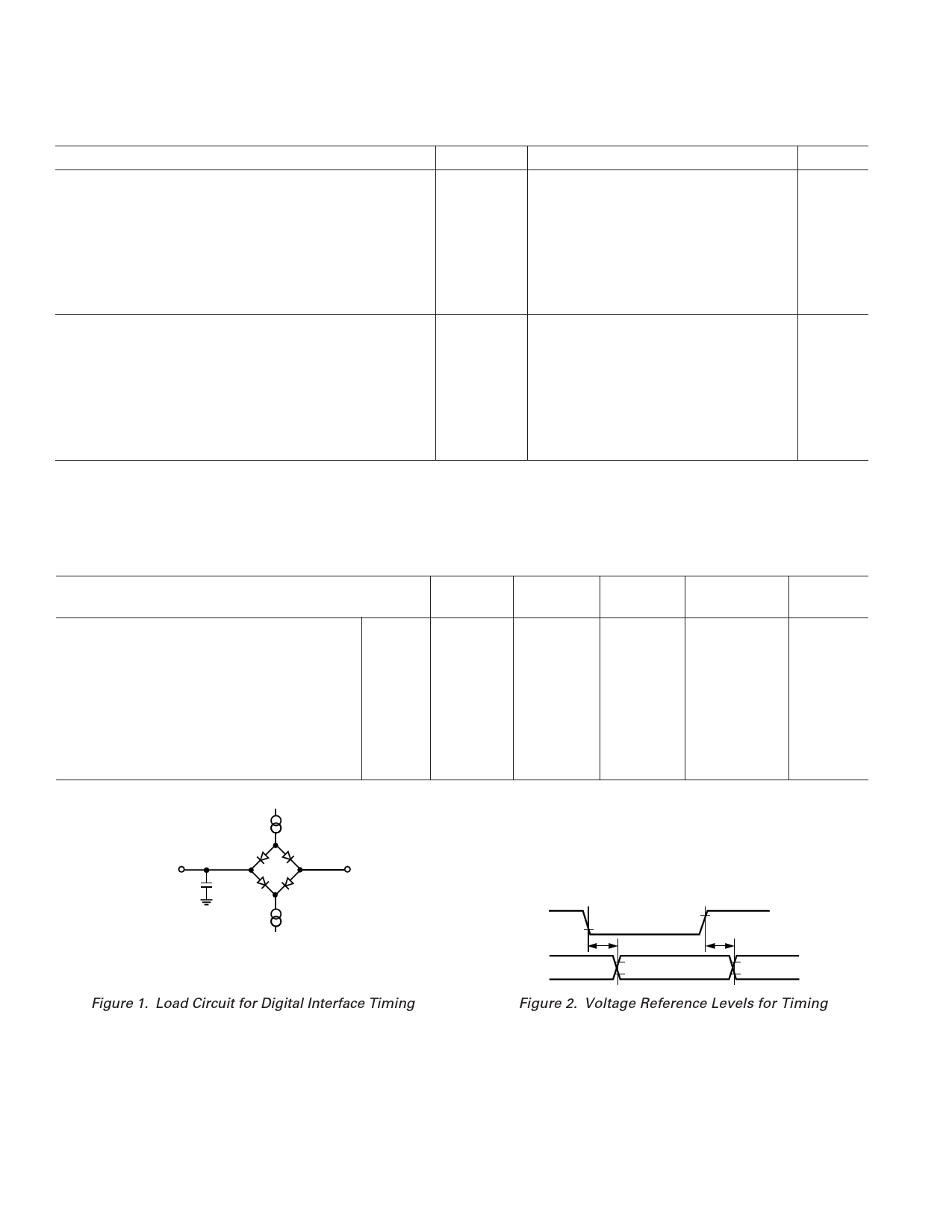
1.6mA IOL
TO OUTPUT
PIN
CL
60pF*
1.4V
500A IOH
*IN SERIAL INTERFACE MODES, THE SYNC, SCLK, AND
SDOUT TIMINGS ARE DEFINED WITH A MAXIMUM LOAD
CL OF 10pF; OTHERWISE, THE LOAD IS 60pF MAXIMUM.
Figure 1. Load Circuit for Digital Interface Timing
0.8V
tDELAY
2V
0.8V
2V
tDELAY
2V
0.8V
Figure 2. Voltage Reference Levels for Timing
–4– REV. B


