No Preview Available !

Dual 10-Bit TxDAC+®
with 2 Interpolation Filters
AD9761
FEATURES
Complete 10-Bit, 40 MSPS Dual Transmit DAC
Excellent Gain and Offset Matching
Differential Nonlinearity Error: 0.5 LSB
Effective Number of Bits: 9.5
Signal-to-Noise and Distortion Ratio: 59 dB
Spurious-Free Dynamic Range: 71 dB
2 Interpolation Filters
20 MSPS/Channel Data Rate
Single Supply: 3 V to 5.5 V
Low Power Dissipation: 93 mW (3 V Supply @
40 MSPS)
On-Chip Reference
28-Lead SSOP
PRODUCT DESCRIPTION
The AD9761 is a complete dual-channel, high speed, 10-bit
CMOS DAC. The AD9761 has been developed specifically for
use in wide bandwidth communication applications (e.g., spread
spectrum) where digital I and Q information is being processed
during transmit operations. It integrates two 10-bit, 40 MSPS
DACs, dual 2 interpolation filters, a voltage reference, and digi-
tal input interface circuitry. The AD9761 supports a 20 MSPS
per channel input data rate that is then interpolated by 2 up to
40 MSPS before simultaneously updating each DAC.
The interleaved I and Q input data stream is presented to the
digital interface circuitry, which consists of I and Q latches as
well as some additional control logic. The data is de-interleaved
back into its original I and Q data. An on-chip state machine
ensures the proper pairing of I and Q data. The data output from
each latch is then processed by a 2 digital interpolation filter
that eases the reconstruction filter requirements. The interpo-
lated output of each filter serves as the input of their respective
10-bit DAC.
The DACs utilize a segmented current source architecture com-
bined with a proprietary switching technique to reduce glitch
energy and to maximize dynamic accuracy. Each DAC provides
differential current output, thus supporting single-ended or dif-
ferential applications. Both DACs are simultaneously updated
and provide a nominal full-scale current of 10 mA. Also, the
full-scale currents between each DAC are matched to within
0.07 dB (i.e., 0.75%), thus eliminating the need for additional
gain calibration circuitry.
The AD9761 is manufactured on an advanced low cost CMOS
process. It operates from a single supply of 3 V to 5.5 V and
consumes 200 mW of power. To make the AD9761 complete, it
also offers an internal 1.20 V temperature-compensated band gap
reference.
FUNCTIONAL BLOCK DIAGRAM
DCOM DVDD CLOCK ACOM AVDD
SLEEP
DAC DATA
INPUTS
(10 BITS)
WRITE INPUT
SELECT INPUT
LATCH
I
2
I
DAC
REFERENCE
LATCH
Q
MUX
CONTROL
BIAS
GENERATOR
2
Q
DAC
AD9761
IOUTA
IOUTB
REFLO
FSADJ
REFIO
COMP1
COMP2
COMP3
QOUTA
QOUTB
PRODUCT HIGHLIGHTS
1. Dual 10-Bit, 40 MSPS DACs
A pair of high performance 40 MSPS DACs optimized for low
distortion performance provide for flexible transmission of I
and Q information.
2. 2 Digital Interpolation Filters
Dual matching FIR interpolation filters with 62.5 dB stop-
band rejection precede each DAC input, thus reducing the
DACs’ reconstruction filter requirements.
3. Low Power
Complete CMOS dual DAC function operates on a low
200 mW on a single supply from 3 V to 5.5 V. The DAC
full-scale current can be reduced for lower power opera-
tion, and a sleep mode is provided for power reduction
during idle periods.
4. On-Chip Voltage Reference
The AD9761 includes a 1.20 V temperature-compensated
band gap voltage reference.
5. Single 10-Bit Digital Input Bus
The AD9761 features a flexible digital interface that allows
each DAC to be addressed in a variety of ways including dif-
ferent update rates.
6. Small Package
The AD9761 offers the complete integrated function in a
compact 28-lead SSOP package.
7. Product Family
The AD9761 Dual Transmit DAC has a pair of Dual Receive
ADC companion products, the AD9281 (8 bits) and AD9201
(10 bits).
REV. C
Information furnished by Analog Devices is believed to be accurate and
reliable. However, no responsibility is assumed by Analog Devices for its
use, nor for any infringements of patents or other rights of third parties
that may result from its use. No license is granted by implication or oth-
erwise under any patent or patent rights of Analog Devices.Trademarks
and registered trademarks are the property of their respective companies.
One Technology Way, P.O. Box 9106, Norwood, MA 02062-9106, U.S.A.
Tel: 781/329-4700
www.analog.com
Fax: 781/326-8703
© 2003 Analog Devices, Inc. All rights reserved.
1 page


AD9761
DIGITAL FILTER SPECIFICATIONS (TMIN to TMAX, AVDD = 2.7 V to 5.5 V, DVDD = 2.7 V to 5.5 V, IOUTFS = 10 mA, unless
otherwise noted.)
Parameter
MAXIMUM INPUT CLOCK RATE (fCLOCK)
DIGITAL FILTER CHARACTERISTICS
Pass Bandwidth1: 0.005 dB
Pass Bandwidth: 0.01 dB
Pass Bandwidth: 0.1 dB
Pass Bandwidth: –3 dB
Linear Phase (FIR Implementation)
Stop-Band Rejection: 0.3 fCLOCK to 0.7 fCLOCK
Group Delay2
Impulse Response Duration3
–40 dB
–60 dB
Min
40
Typ
0.2010
0.2025
0.2105
0.239
–62.5
32
28
40
Max
Unit
MSPS
fOUT/fCLOCK
fOUT/fCLOCK
fOUT/fCLOCK
fOUT/fCLOCK
dB
Input Clock Cycles
Input Clock Cycles
Input Clock Cycles
NOTES
1Excludes SINx/x characteristic of DAC.
2Defined as the number of data clock cycles between impulse input and peak of output response.
355 input clock periods from input to I DAC, 56 to Q DAC. Propagation delay is delay from data input to DAC update.
Specifications subject to change without notice.
0
–20
–40
–60
–80
–100
–120 0
0.1 0.2 0.3 0.4
FREQUENCY RESPONSE (DC to fCLOCK/2)
0.5
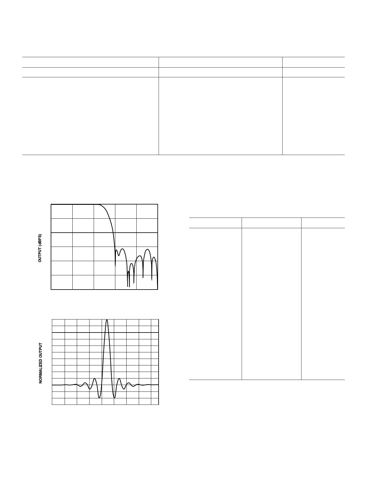
Figure 2a. FIR Filter Frequency Response
1
0.9
0.8
0.7
0.6
0.5
0.4
0.3
0.2
0.1
0
–0.1
–0.2
–0.3 0
5 10 15 20 25 30 35 40
TIME (Samples)
Figure 2b. FIR Filter Impulse Response
Table I. Integer Filter Coefficients for 43-Tap Half-Band
FIR Filter
Lower Coefficient Upper Coefficient Integer Value
H(1)
H(2)
H(3)
H(4)
H(5)
H(6)
H(7)
H(8)
H(9)
H(10)
H(11)
H(12)
H(13)
H(14)
H(15)
H(16)
H(17)
H(18)
H(19)
H(20)
H(21)
H(22)
H(43)
H(42)
H(41)
H(40)
H(39)
H(38)
H(37)
H(36)
H(35)
H(34)
H(33)
H(32)
H(31)
H(30)
H(29)
H(28)
H(27)
H(26)
H(25)
H(24)
H(23)
1
0
–3
0
8
0
–16
0
29
0
–50
0
81
0
–131
0
216
0
–400
0
1264
1998
–4– REV. C
5 Page


AD9761
FUNCTIONAL DESCRIPTION
Figure 4 shows a simplified block diagram of the AD9761. The
AD9761 is a complete dual-channel, high speed, 10-bit CMOS
DAC capable of operating up to a 40 MHz clock rate. It has
been optimized for the transmit section of wideband communica-
tion systems employing I and Q modulation schemes. Excellent
matching characteristics between channels reduce the need for
any external calibration circuitry. Dual matching 2 interpola-
tion filters included in the I and Q data path simplify any post
band-limiting filter requirements. The AD9761 interfaces with a
single 10-bit digital input bus that supports interleaved I and Q
input data.
DCOM DVDD CLOCK ACOM AVDD
SLEEP
DAC DATA
INPUTS
(10 BITS)
WRITE INPUT
SELECT INPUT
LATCH
I
2
I
DAC
REFERENCE
LATCH
Q
MUX
CONTROL
BIAS
GENERATOR
2
Q
DAC
AD9761
IOUTA
IOUTB
REFLO
FSADJ
REFIO
COMP1
COMP2
COMP3
QOUTA
QOUTB
Figure 4. Dual DAC Functional Block Diagram
Referring to Figure 4, the AD9761 consists of an analog sec-
tion and a digital section. The analog section includes matched
I and Q 10-bit DACs, a 1.20 V band gap voltage reference, and
a reference control amplifier.The digital section includes two 2
interpolation filters, segment decoding logic, and some additional
digital input interface circuitry. The analog and digital sections of
the AD9761 have separate power supply inputs (i.e., AVDD and
DVDD) that can operate independently. The digital supply can
operate over a 2.7 V to 5.5 V range, allowing it to accommodate
TTL as well as 3.3 V and 5 V CMOS logic families. The analog
supply must be restricted from 3.0 V to 5.5 V to maintain opti-
mum performance.
Each DAC consists of a large PMOS current source array capable
of providing up to 10 mA of full-scale current, IOUTFS. Each array is
divided into 15 equal currents that make up the four most signifi-
cant bits (MSBs). The next four bits or middle bits consist of 15
equal current sources whose values are 1/16 of an MSB current
source. The remaining LSBs are binary weighted fractions of
the middle bits’ current sources. All of these current sources are
switched to one of two output nodes (i.e., IOUTA or IOUTB)
via PMOS differential current switches.
The full-scale output current, IOUTFS, of each DAC is regulated
from the same voltage reference and control amplifier, thus
ensuring excellent gain matching and drift characteristics
between DACs. IOUTFS can be set from 1 mA to 10 mA via an
external resistor, RSET. The external resistor in combination
with both the reference control amplifier and voltage reference,
VREFIO, sets the reference current, IREF, which is mirrored over
to the segmented current sources with the proper scaling factor.
IOUTFS is exactly 16 times the value of IREF.
The I and Q DACs are simultaneously updated on the rising
edge of CLOCK with digital data from their respective 2
digital interpolation filters. The 2 interpolation filters essen-
tially multiply the input data rate of each DAC by a factor of
2, relative to its original input data rate, while simultaneously
reducing the magnitude of the first image associated with the
DAC’s original input data rate. Since the AD9761 supports a
single 10-bit digital bus with interleaved I and Q input data, the
original I and Q input data rate before interpolation is one-half
the CLOCK rate. After interpolation, the data rate into each I
and Q DAC becomes equal to the CLOCK rate.
The benefits of an interpolation filter are illustrated in Figure 5,
which shows an example of the frequency and time domain rep-
resentation of a discrete time sine wave signal before and after
it is applied to a digital interpolation filter. Images of the sine
wave signal appear around multiples of the DAC’s input data
rate as predicted by the sampling theory. These undesirable
images will also appear at the output of a reconstruction DAC,
although modified by the DAC’s sin(x)/(x) response. In many
band-limited applications, these images must be suppressed by
an analog filter following the DAC. The complexity of this ana-
TIME DOMAIN
2
fCLOCK
FUNDAMENTAL 1ST IMAGE
FREQUENCY DOMAIN
fCLOCK
2
fCLOCK
1
fCLOCK
FUNDAMENTAL DIGITAL
FILTER
NEW
1ST IMAGE
SUPPRESSED
OLD
fCLOCK
1ST IMAGE
2
fCLOCK
DACs
SIN(X)
X
fCLOCK
2
fCLOCK
INPUT DATA LATCH
2 INTERPOLATION FILTER
2
DAC
fCLOCK
2
fCLOCK
Figure 5.Time and Frequency Domain Example of Digital Interpolation Filter
–10–
REV. C
11 Page
| 


