|
|
PDF Am29F040 Data sheet ( Hoja de datos )
| Número de pieza | Am29F040 | |
| Descripción | 4 Megabit CMOS 5.0 Volt-only Sector Erase Flash Memory | |
| Fabricantes | AMD | |
| Logotipo |  |
|
Hay una vista previa y un enlace de descarga de Am29F040 (archivo pdf) en la parte inferior de esta página. Total 30 Páginas | ||
|
No Preview Available !
FINAL
Am29F040
4 Megabit (524,288 x 8-Bit) CMOS 5.0 Volt-only,
Sector Erase Flash Memory
DISTINCTIVE CHARACTERISTICS
s 5.0 V ± 10% for read and write operations
— Minimizes system level power requirements
s Compatible with JEDEC-standards
— Pinout and software compatible with single-
power-supply Flash
— Superior inadvertent write protection
s Package options
— 32-pin PLCC
— 32-pin TSOP
— 32-pin PDIP
s Minimum 100,000 write/erase cycles guaranteed
s High performance
— 55 ns maximum access time
s Sector erase architecture
— Uniform sectors of 64 Kbytes each
— Any combination of sectors can be erased.
Also supports full chip erase.
s Sector protection
— Hardware method that disables any combination
of sectors from write or erase operations
s Embedded Erase Algorithms
— Automatically preprograms and erases the chip
or any combination of sectors
s Embedded Program Algorithms
— Automatically programs and verifies data at
specified address
s Data Polling and Toggle Bit feature for detection
of program or erase cycle completion
s Erase suspend/resume
— Supports reading data from a sector not being
erased
s Low power consumption
— 20 mA typical active read current
— 30 mA typical program/erase current
s Enhanced power management for standby
mode
— <1 µA typical standby current
— Standard access time from standby mode
GENERAL DESCRIPTION
The Am29F040 is a 4 Mbit, 5.0 Volt-only Flash memory
organized as 512 Kbytes of 8 bits each. The Am29F040
is offered in a 32-pin package. This device is designed
to be programmed in-system with the standard system
5.0 V VCC supply. A 12.0 V VPP is not required for
write or erase operations. The device can also be
reprogrammed in standard EPROM programmers.
The standard Am29F040 offers access times between
55 ns and 150 ns, allowing operation of high-speed
microprocessors without wait states. To eliminate bus
contention the device has separate chip enable (CE),
write enable (WE) and output enable (OE) controls.
The Am29F040 is entirely command set compatible
with the JEDEC single-power-supply Flash standard.
Commands are written to the command register using
standard microprocessor write timings. Register con-
tents serve as input to an internal state machine
which controls the erase and programming circuitry.
Write cycles also internally latch addresses and data
needed for the programming and erase operations.
Reading data out of the device is similar to reading
from 12.0 Volt Flash or EPROM devices.
The Am29F040 is programmed by executing the pro-
gram command sequence. This will invoke the Embed-
ded Program Algorithm which is an internal algorithm
that automatically times the program pulse widths and
verifies proper cell margin. Typically, each sector can
be programmed and verified in less than one second.
Erase is accomplished by executing the erase com-
mand sequence. This will invoke the Embedded Erase
Algorithm which is an internal algorithm that automati-
cally preprograms the array if it is not already pro-
grammed before executing the erase operation. During
erase, the device automatically times the erase pulse
widths and verifies proper cell margin.
Publication# 17113 Rev: E Amendment/0
Issue Date: November 1996
1 page 
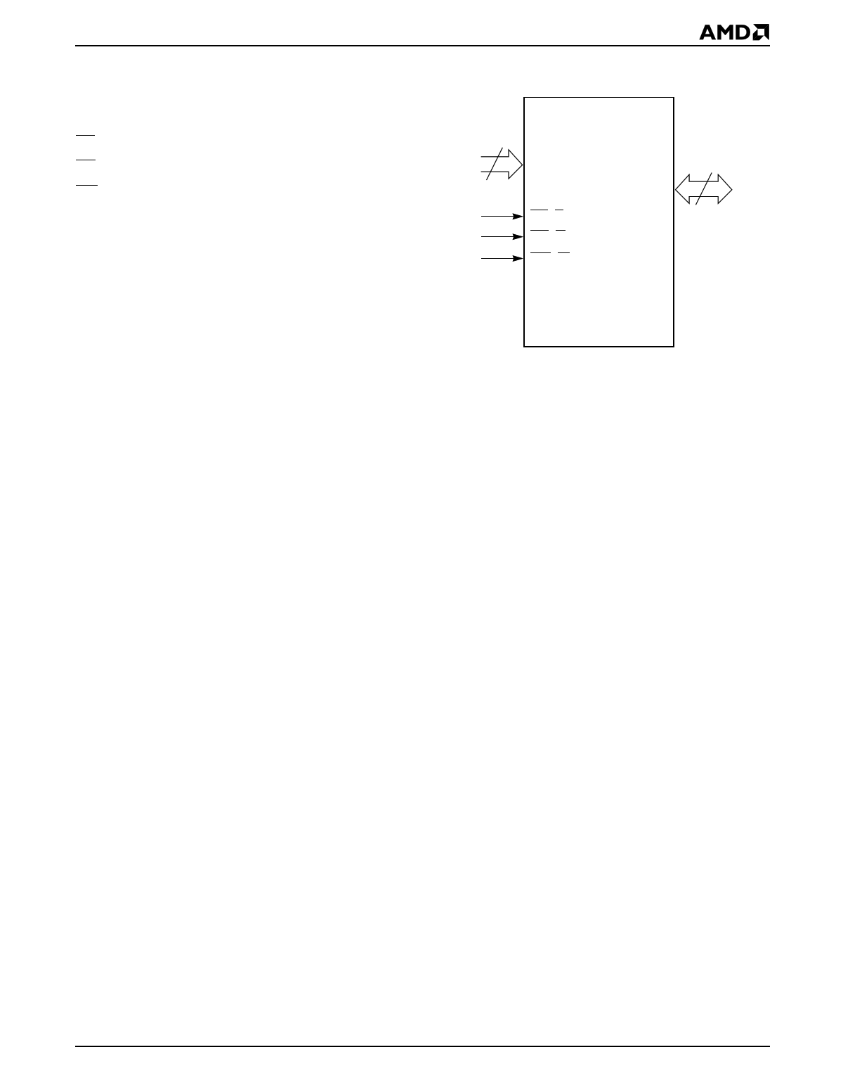
PIN CONFIGURATION
A0–A18 = Address Inputs
DQ0–DQ7 = Data Input/Output
CE = Chip Enable
OE = Output Enable
WE = Write Enable
VSS = Device Ground
VCC = Device Power Supply
(5.0 V ±10% or ±5%)
LOGIC SYMBOL
19
A0–A18
CE (E)
OE (G)
WE (W)
DQ0–DQ7
8
17113E-6
Am29F040
5
5 Page 
Erase Suspend
The Erase Suspend command allows the user to inter-
rupt a Sector Erase operation and then perform data
reads from a sector not being erased. This command is
applicable ONLY during the Sector Erase operation
which includes the time-out period for sector erase. The
Erase Suspend command will be ignored if written dur-
ing the Chip Erase operation or Embedded Program Al-
gorithm. Writing the Erase Suspend command during
the Sector Erase time-out results in immediate termina-
tion of the time-out period and suspension of the erase
operation.
Any other command written during the Erase Sus-
pend mode will be ignored except the Erase Resume
command. Writing the Erase Resume command
resumes the erase operation. The addresses are
“don’t-cares” when writing the Erase Suspend or
Erase Resume command.
When the Erase Suspend command is written during
the Sector Erase operation, the device will take a max-
imum of 15 µs to suspend the erase operation. When
the device has entered the erase-suspended mode,
DQ7 bit will be at logic “1”, and DQ6 will stop toggling.
The user must use the address of the erasing sector for
reading DQ6 and DQ7 to determine if the erase opera-
tion has been suspended. Further writes of the Erase
Suspend command are ignored.
When the erase operation has been suspended, the
device defaults to the erase-suspend-read mode.
Reading data in this mode is the same as reading from
the standard read mode except that the data must be
read from sectors that have not been erase-suspended.
To resume the operation of Sector Erase, the Resume
command (30H) should be written. Any further writes of
the Resume command at this point will be ignored. An-
other Erase Suspend command can be written after the
chip has resumed erasing.
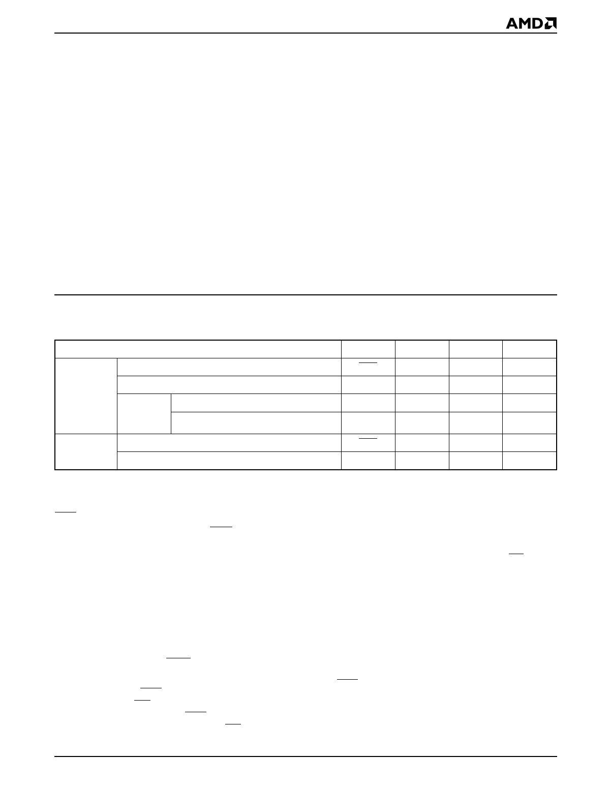
Write Operation Status
Table 5. Write Operation Status
Status
DQ7
Byte Programming in Embedded Algorithm
DQ7
In Progress
Embedded Erase Algorithm
Erase
Erase Suspended Sector
Suspended
Mode
Non-Erase Suspended Sector
0
1
Data
Exceeded Byte-Programming in Embedded Algorithm
Time Limits Embedded Erase Algorithm
DQ7
0
DQ6
Toggle
Toggle
No Toggle
Data
Toggle
Toggle
DQ5
0
0
0
Data
1
1
DQ3
0
1
1
Data
0
1
DQ7
Data Polling
The Am29F040 device features Data Polling as a
method to indicate to the host that the Embedded
Algorithms are in progress or completed. During the
Embedded Program Algorithm an attempt to read the
device produces the compliment of the data last written
to DQ7. Upon completion of the Embedded Program
Algorithm, reading the device produces the true data
last written to DQ7. During the Embedded Erase Algo-
rithm, reading the device produces a “0” at the DQ7
output. Upon completion of the Embedded Erase Algo-
rithm, reading the device produces a “1” at the DQ7
output. The flowchart for Data Polling (DQ7) is shown
in Figure 3.
For chip erase, the Data Polling is valid after the rising
edge of the sixth WE pulse in the six write pulse se-
quence. For sector erase, the Data Polling is valid after
the last rising edge of the sector erase WE pulse. Data
Polling must be performed at sector address within any
of the sectors being erased and not a protected sector.
Otherwise, the status may not be valid. Once the Em-
bedded Algorithm operation is close to being com-
pleted, the Am29F040 data pins (DQ7) may change
asynchronously while the output enable (OE) is as-
serted low. This means that the device is driving status
information on DQ7 at one instant of time and then that
byte’s valid data at the next instant of time. Depending
on when the system samples the DQ7 output, it may
read the status or valid data. Even if the device has
completed the Embedded Algorithm operation and
DQ7 has a valid data, the data outputs on DQ0–DQ6
may be still invalid. The valid data on DQ0–DQ7 will be
read on the successive read attempts.
The Data Polling feature is active during the Embedded
Programming Algorithm, Embedded Erase Algorithm,
Erase Suspend, or sector erase time-out (see Table 5).
Am29F040
11
11 Page | ||
| Páginas | Total 30 Páginas | |
| PDF Descargar | [ Datasheet Am29F040.PDF ] | |
Hoja de datos destacado
| Número de pieza | Descripción | Fabricantes |
| Am29F040 | 4 Megabit CMOS 5.0 Volt-only Sector Erase Flash Memory | AMD |
| AM29F040B | 4 Megabit CMOS 5.0 Volt-only Uniform Sector Flash Memory | AMD |
| Número de pieza | Descripción | Fabricantes |
| SLA6805M | High Voltage 3 phase Motor Driver IC. |
Sanken |
| SDC1742 | 12- and 14-Bit Hybrid Synchro / Resolver-to-Digital Converters. |
Analog Devices |
|
DataSheet.es es una pagina web que funciona como un repositorio de manuales o hoja de datos de muchos de los productos más populares, |
| DataSheet.es | 2020 | Privacy Policy | Contacto | Buscar |
