|
|
|
PDF LTC2328-16 Data sheet ( Hoja de datos )
| Número de pieza | LTC2328-16 | |
| Descripción | Pseudo-Differential Input ADC | |
| Fabricantes | Linear Technology | |
| Logotipo | ||
Hay una vista previa y un enlace de descarga de LTC2328-16 (archivo pdf) en la parte inferior de esta página. Total 26 Páginas | ||
|
No Preview Available !
LTC2328-16
16-Bit, 1Msps, ±10.24V
True Bipolar, Pseudo-Differential
Input ADC with 93.5dB SNR
Features
Description
nn 1Msps Throughput Rate
nn ±1.5LSB INL (Max)
nn Guaranteed 16-Bit No Missing Codes
nn Pseudo-Differential Inputs
nn True Bipolar Input Ranges ±6.25V, ±10.24V, ±12.5V
nn 93.5dB SNR (Typ) at fIN = 2kHz
nn –111dB THD (Typ) at fIN = 2kHz
nn Guaranteed Operation to 125°C
nn Single 5V Supply
nn Low Drift (20ppm/°C Max) 2.048V Internal Reference
nn Onboard Single-Shot Capable Reference Buffer
nn No Pipeline Delay, No Cycle Latency
nn 1.8V to 5V I/O Voltages
nn SPI-Compatible Serial I/O with Daisy-Chain Mode
nn Internal Conversion Clock
nn Power Dissipation 50mW (Typ)
nn 16-Lead MSOP Package
Applications
nn Programmable Logic Controllers
nn Industrial Process Control
nn High Speed Data Acquisition
nn Portable or Compact Instrumentation
nn ATE
The LTC®2328-16 is a low noise, high speed 16-bit suc-
cessive approximation register (SAR) ADC with pseudo-
differential inputs. Operating from a single 5V supply, the
LTC2328-16 has a ±10.24V true bipolar input range, making
it ideal for high voltage applications which require a wide
dynamic range. The LTC2328-16 achieves ±1.5LSB INL
maximum, no missing codes at 16 bits with 93.5dB SNR.
The LTC2328-16 has an onboard single-shot capable
reference buffer and low drift (20ppm/°C max) 2.048V
temperature compensated reference. The LTC2328-16
also has a high speed SPI-compatible serial interface that
supports 1.8V, 2.5V, 3.3V and 5V logic while also featur-
ing a daisy-chain mode. The fast 1Msps throughput with
no cycle latency makes the LTC2328-16 ideally suited
for a wide variety of high speed applications. An internal
oscillator sets the conversion time, easing external timing
considerations. The LTC2328-16 dissipates only 50mW
and automatically naps between conversions, leading to
reduced power dissipation that scales with the sampling
rate. A sleep mode is also provided to reduce the power
consumption of the LTC2328-16 to 300μW for further
power savings during inactive periods.
L, LT, LTC, LTM, Linear Technology and the Linear logo are registered trademarks and
SoftSpan is a trademark of Linear Technology Corporation. All other trademarks are the
property of their respective owners. Protected by U.S. Patents, including 7705765, 7961132.
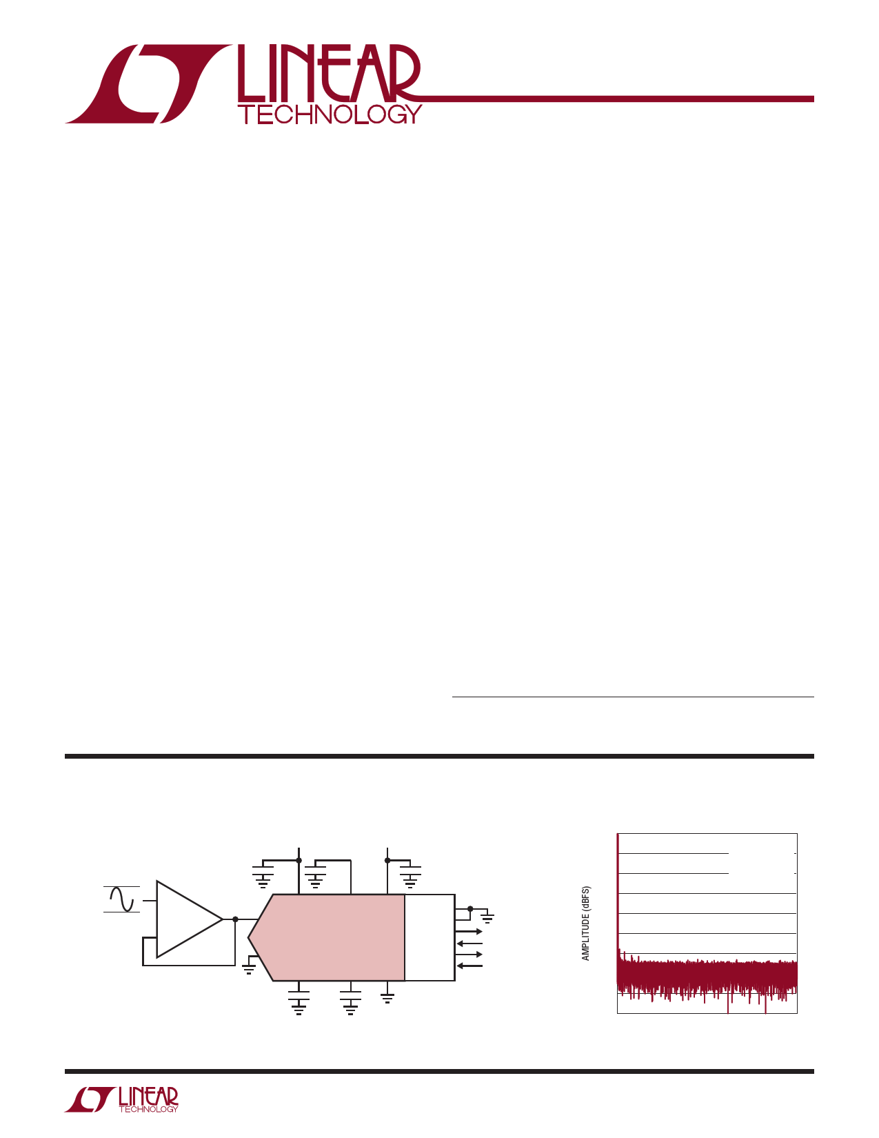
Typical Application
+10.24V
–10.24V
+
LT®1468
–
5V
10µF
1.8V TO 5V
2.2µF
0.1µF
VDD
IN+
VDDLBYP OVDD
LTC2328-16
IN–
RERFEBFUF
REFIN
GND
47µF
100nF
CHAIN
RDL/SDI
SDO
SCK
BUSY
CNV
232816 TA01a
SAMPLE CLOCK
For more information www.linear.com/LTC2328-16
32k Point FFT fS = 1Msps,
fIN = 2kHz
0 SNR = 93.5dB
–20 THD = –111dB
SINAD = 93.4dB
–40 SFDR = –115dB
–60
–80
–100
–120
–140
–160
–180
0
100 200 300 400 500
FREQUENCY (kHz)
232816 TA01b
232816fb
1
1 page 
LTC2328-16
A DC Timing Characteristics The l denotes the specifications which apply over the full operating
temperature range, otherwise specifications are at TA = 25°C. (Note 4)
SYMBOL PARAMETER
CONDITIONS
MIN TYP MAX UNITS
fSMPL
tCONV
tACQ
tCYC
tCNVH
tBUSYLH
tCNVL
tQUIET
tSCK
tSCKH
tSCKL
tSSDISCK
tHSDISCK
tSCKCH
tDSDO
Maximum Sampling Frequency
Conversion Time
Acquisition Time
Time Between Conversions
CNV High Time
CNV↑ to BUSY Delay
Minimum Low Time for CNV
SCK Quiet Time from CNV↑
SCK Period
SCK High Time
SCK Low Time
SDI Setup Time From SCK↑
SDI Hold Time From SCK↑
SCK Period in Chain Mode
SDO Data Valid Delay from SCK↑
tHSDO
tDSDOBUSYL
tEN
tDIS
tWAKE
SDO Data Remains Valid Delay from SCK↑
SDO Data Valid Delay from BUSY↓
Bus Enable Time After RDL↓
Bus Relinquish Time After RDL↑
REFBUF Wake-Up Time
tACQ = tCYC – tCONV – tBUSYLH (Note 11)
CL = 20pF
(Note 12)
(Note 11)
(Notes 12, 13)
(Note 12)
(Note 12)
tSCKCH = tSSDISCK + tDSDO (Note 12)
CL = 20pF, OVDD = 5.25V
CL = 20pF, OVDD = 2.5V
CL = 20pF, OVDD = 1.71V
CL = 20pF (Note 11)
CL = 20pF (Note 11)
(Note 12)
(Note 12)
CREFBUF = 47μF, CREFIN = 100nF
l 1 Msps
l 460
527 ns
l 460
ns
l1
µs
l 20
ns
l 13 ns
l 20
ns
l 20
ns
l 10
ns
l4
ns
l4
ns
l4
ns
l1
ns
l 13.5
ns
l 7.5 ns
l 8 ns
l 9.5 ns
l1
ns
l 5 ns
l 16 ns
l 13 ns
200 ms
Note 1: Stresses beyond those listed under Absolute Maximum Ratings
may cause permanent damage to the device. Exposure to any Absolute
Maximum Rating condition for extended periods may affect device
reliability and lifetime.
Note 2: All voltage values are with respect to ground.
Note 3: When these pin voltages are taken below ground or above VDD or
OVDD, they will be clamped by internal diodes. This product can handle
input currents up to 100mA below ground or above VDD or OVDD without
latch-up.
Note 4: VDD = 5V, OVDD = 2.5V, ±10.24V Range, REFIN = 2.048V,
fSMPL = 1MHz.
Note 5: Recommended operating conditions.
Note 6: Integral nonlinearity is defined as the deviation of a code from a
straight line passing through the actual endpoints of the transfer curve.
The deviation is measured from the center of the quantization band.
Note 7: Bipolar zero error is the offset voltage measured from –0.5LSB
when the output code flickers between 0000 0000 0000 0000 and 1111
1111 1111 1111. Full-scale bipolar error is the worst-case of –FS or +FS
untrimmed deviation from ideal first and last code transitions and includes
the effect of offset error.
Note 8: All specifications in dB are referred to a full-scale ±10.24V input
with REFIN = 2.048V.
Note 9: When REFBUF is overdriven, the internal reference buffer must be
turned off by setting REFIN = 0V.
Note 10: fSMPL = 1MHz, IREFBUF varies proportionally with sample rate.
Note 11: Guaranteed by design, not subject to test.
Note 12: Parameter tested and guaranteed at OVDD = 1.71V, OVDD = 2.5V
and OVDD = 5.25V.
Note 13: tSCK of 10ns maximum allows a shift clock frequency up to
100MHz for rising edge capture.
Note 14: Temperature coefficient is calculated by dividing the maximum
change in output voltage by the specified temperature range.
0.8 • OVDD
tDELAY
0.8 • OVDD
0.2 • OVDD
0.2 • OVDD
tDELAY
0.8 • OVDD
0.2 • OVDD
50%
tWIDTH
Figure 1. Voltage Levels for Timing Specifications
50%
232816 F01
For more information www.linear.com/LTC2328-16
232816fb
5
5 Page 
LTC2328-16
Applications Information
a total impedance of 2kΩ. The resistor divider network
attenuates and level shifts the ±2.5 • REFBUF true bipolar
signal swing of each input to the 0-REFBUF input signal
swing of the ADC core. In the acquisition phase, 45pF (CIN)
from the sampling CDAC in series with approximately 50Ω
(RON) from the on-resistance of the sampling switch is
connected to the output of the resistor divider network.
Any unwanted signal that is common to both inputs will
be reduced by the common mode rejection of the ADC
core and resistor divider network. The IN+ input of the
ADC core draws a current spike while charging the CIN
capacitor during acquisition.
Input Drive Circuits
A low impedance source can directly drive the high im-
pedance input of the LTC2328-16 without gain error. A
high impedance source should be buffered to minimize
settling time during acquisition and to optimize the dis-
tortion performance of the ADC. Minimizing settling time
is important even for DC inputs, because the ADC input
draws a current spike when entering acquisition.
For best performance, a buffer amplifier should be used
to drive the analog input of the LTC2328-16. The amplifier
provides low output impedance to minimize gain error
and allows for fast settling of the analog signal during
the acquisition phase. It also provides isolation between
the signal source and the ADC input which draws a small
current spike during acquisition.
Input Filtering
The noise and distortion of the buffer amplifier and signal
source must be considered since they add to the ADC noise
and distortion. Noisy input signals should be filtered prior
to the buffer amplifier input with a low bandwidth filter to
minimize noise. The simple 1-pole RC lowpass filter shown
in Figure 4 is sufficient for many applications.
The input resistor divider network, sampling switch on-
resistance (RON) and the sample capacitor (CIN) form a
second lowpass filter that limits the input bandwidth to
the ADC core to 7MHz. A buffer amplifier with a low noise
density must be selected to minimize the degradation of
the SNR over this bandwidth.
±10.24V
50Ω
66nF
BW = 48kHz
+
LT1468
–
IN+
LTC2328-16
IN–
Figure 4. Input Signal Chain
232816 F04
High quality capacitors and resistors should be used in the
RC filters since these components can add distortion. NPO
and silver mica type dielectric capacitors have excellent
linearity. Carbon surface mount resistors can generate
distortion from self heating and from damage that may
occur during soldering. Metal film surface mount resistors
are much less susceptible to both problems.
Pseudo-Differential Bipolar Inputs
For most applications, we recommend the low power
LT1468 ADC driver to drive the LTC2328-16. With a low
noise density of 5nV/√Hz and a low supply current of 3mA,
the LT1468 is flexible and may be configured to convert
signals of various amplitudes to the ±10.24V input range
of the LTC2328-16.
To achieve the full distortion performance of the
LTC2328‑16, a low distortion single-ended signal source
driven through the LT1468 configured as a unity-gain
buffer as shown in Figure 4 can be used to get the full
data sheet THD specification of –111dB.
ADC Reference
There are three ways of providing the ADC reference. The
first is to use both the internal reference and reference
buffer. The second is to externally overdrive the internal
reference and use the internal reference buffer. The third
is to disable the internal reference buffer and overdrive
the REFBUF pin from an external source. The following
tables give examples of these cases and the resulting
bipolar input ranges.
For more information www.linear.com/LTC2328-16
232816fb
11
11 Page | ||
| Páginas | Total 26 Páginas | |
| PDF Descargar | [ Datasheet LTC2328-16.PDF ] | |
Hoja de datos destacado
| Número de pieza | Descripción | Fabricantes |
| LTC2328-16 | Pseudo-Differential Input ADC | Linear Technology |
| LTC2328-18 | Pseudo-Differential Input ADC | Linear Technology |
| Número de pieza | Descripción | Fabricantes |
| SLA6805M | High Voltage 3 phase Motor Driver IC. |
Sanken |
| SDC1742 | 12- and 14-Bit Hybrid Synchro / Resolver-to-Digital Converters. |
Analog Devices |
|
DataSheet.es es una pagina web que funciona como un repositorio de manuales o hoja de datos de muchos de los productos más populares, |
| DataSheet.es | 2020 | Privacy Policy | Contacto | Buscar |