|
|
|
PDF LTC2327-18 Data sheet ( Hoja de datos )
| Número de pieza | LTC2327-18 | |
| Descripción | Pseudo-Differential Input ADC | |
| Fabricantes | Linear Technology | |
| Logotipo | ||
Hay una vista previa y un enlace de descarga de LTC2327-18 (archivo pdf) en la parte inferior de esta página. Total 26 Páginas | ||
|
No Preview Available !
LTC2327-18
Features
18-Bit, 500ksps, ±10.24V
True Bipolar, Pseudo-Differential
Input ADC with 95dB SNR
Description
nn 500ksps Throughput Rate
nn ±5LSB INL (Max)
nn Guaranteed 18-Bit No Missing Codes
nn Pseudo-Differential Inputs
nn True Bipolar Input Ranges ±6.25V, ±10.24V, ±12.5V
nn 95dB SNR (Typ) at fIN = 2kHz
nn –111dB THD (Typ) at fIN = 2kHz
nn Guaranteed Operation to 125°C
nn Single 5V Supply
nn Low Drift (20ppm/°C Max) 2.048V Internal Reference
nn Onboard Single-Shot Capable Reference Buffer
nn No Pipeline Delay, No Cycle Latency
nn 1.8V to 5V I/O Voltages
nn SPI-Compatible Serial I/O with Daisy-Chain Mode
nn Internal Conversion Clock
nn Power Dissipation 36mW (Typ)
nn 16-Lead MSOP Package
Applications
nn Programmable Logic Controllers
nn Industrial Process Control
nn High Speed Data Acquisition
nn Portable or Compact Instrumentation
nn ATE
The LTC®2327-18 is a low noise, high speed 18-bit suc-
cessive approximation register (SAR) ADC with pseudo-
differential inputs. Operating from a single 5V supply,
the LTC2327-18 has a ±10.24V true bipolar input range,
making it ideal for high voltage applications which require
a wide dynamic range. The LTC2327-18 achieves ±5LSB
INL maximum, no missing codes at 18 bits with 95dB SNR.
The LTC2327-18 has an onboard single-shot capable
reference buffer and low drift (20ppm/°C max) 2.048V
temperature compensated reference. The LTC2327-18
also has a high speed SPI-compatible serial interface that
supports 1.8V, 2.5V, 3.3V and 5V logic while also featuring
a daisy-chain mode. The fast 500ksps throughput with
no cycle latency makes the LTC2327-18 ideally suited
for a wide variety of high speed applications. An internal
oscillator sets the conversion time, easing external timing
considerations. The LTC2327-18 dissipates only 36mW
and automatically naps between conversions, leading to
reduced power dissipation that scales with the sampling
rate. A sleep mode is also provided to reduce the power
consumption of the LTC2327-18 to 300μW for further
power savings during inactive periods.
L, LT, LTC, LTM, Linear Technology and the Linear logo are registered trademarks and
SoftSpan is a trademark of Linear Technology Corporation. All other trademarks are the
property of their respective owners. Protected by U.S. Patents, including 7705765, 7961132.
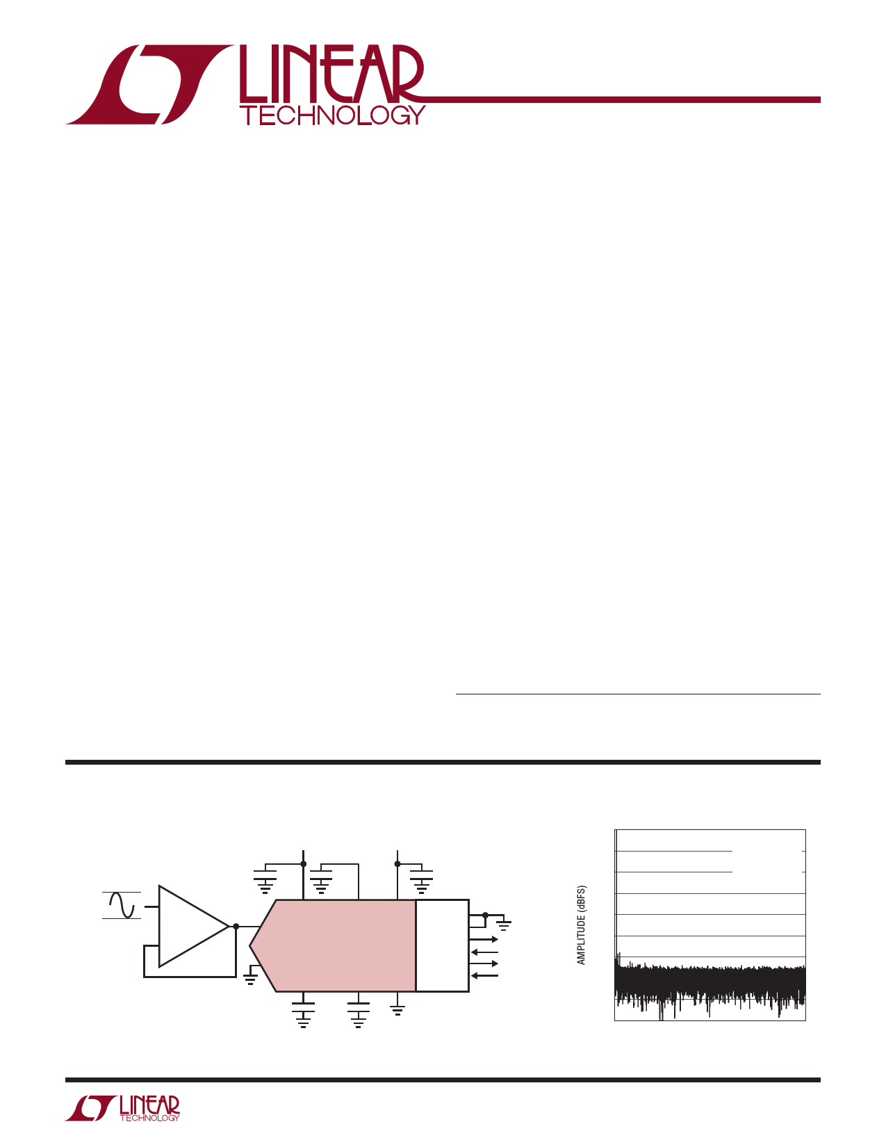
Typical Application
+10.24V
–10.24V
+
LT®1468
–
5V
10µF
1.8V TO 5V
2.2µF
0.1µF
VDD
IN+
VDDLBYP OVDD
LTC2327-18
IN–
RERFEBFUF
REFIN
GND
47µF
100nF
CHAIN
RDL/SDI
SDO
SCK
BUSY
CNV
232718 TA01
SAMPLE CLOCK
For more information www.linear.com/LTC2327-18
0
–20
–40
–60
–80
–100
–120
–140
–160
–180
0
32k Point FFT fS = 500ksps,
fIN = 2kHz
SNR = 95.3dB
THD = –113dB
SINAD = 95.2dB
SFDR = –116dB
50 100 150 200 250
FREQUENCY (kHz)
232718 TA01b
232718fb
1
1 page 
LTC2327-18
Power Requirements The l denotes the specifications which apply over the full operating temperature
range, otherwise specifications are at TA = 25°C. (Note 4)
SYMBOL
PARAMETER
CONDITIONS
MIN TYP
MAX UNITS
VDD
OVDD
IVDD
IIONVADPD
ISLEEP
PD
Supply Voltage
l 4.75
5
5.25
V
Supply Voltage
l 1.71
5.25 V
Supply Current
Supply Current
Nap Mode Current
Sleep Mode Current
Power Dissipation
Nap Mode
Sleep Mode
500ksps Sample Rate (IN+ = –10.24V, IN– = 0V)
500ksps Sample Rate (IN+ = IN– = 0V)
5C0o0nkvseprssioSnamDopnleeR(IaVtDeD(C+LIO=V2D0Dp, FIN) + = –10.24V, IN– = 0V)
Sleep Mode (IVDD + IOVDD)
500ksps Sample Rate (IN+ = –10.24V, IN– = 0V)
500ksps Sample Rate (IN+ = IN– = 0V)
Conversion Done (IVDD + IOVDD, IN+ = –10.24V, IN– = 0V)
Sleep Mode (IVDD + IOVDD)
l
l
l
l
l
l
11.4 14
7.2
0.1
8.4 10
60 225
mA
mA
mA
mA
μA
57 70 mW
36 mW
42 50 mW
0.3 1.1 mW
A DC Timing Characteristics The l denotes the specifications which apply over the full operating
temperature range, otherwise specifications are at TA = 25°C. (Note 4)
SYMBOL PARAMETER
CONDITIONS
MIN TYP MAX UNITS
fSMPL
tCONV
tACQ
tHOLD
tCYC
tCNVH
tBUSYLH
tCNVL
tQUIET
tSCK
tSCKH
tSCKL
tSSDISCK
tHSDISCK
tSCKCH
tDSDO
Maximum Sampling Frequency
Conversion Time
Acquisition Time
Maximum Time between Acquisitions
Time Between Conversions
CNV High Time
CNV↑ to BUSY Delay
Minimum Low Time for CNV
SCK Quiet Time from CNV↑
SCK Period
SCK High Time
SCK Low Time
SDI Setup Time From SCK↑
SDI Hold Time From SCK↑
SCK Period in Chain Mode
SDO Data Valid Delay from SCK↑
tHSDO
tDSDOBUSYL
tEN
tDIS
tWAKE
SDO Data Remains Valid Delay from SCK↑
SDO Data Valid Delay from BUSY↓
Bus Enable Time After RDL↓
Bus Relinquish Time After RDL↑
REFBUF Wakeup Time
tACQ = tCYC – tHOLD (Note 11)
CL = 20pF
(Note 12)
(Note 11)
(Notes 12, 13)
(Note 12)
(Note 12)
tSCKCH = tSSDISCK + tDSDO (Note 12)
CL = 20pF, OVDD = 5.25V
CL = 20pF, OVDD = 2.5V
CL = 20pF, OVDD = 1.71V
CL = 20pF (Note 11)
CL = 20pF (Note 11)
(Note 12)
(Note 12)
CREFBUF = 47μF, CREFIN = 100nF
l 500 ksps
l1
1.5 µs
l 1.460
µs
l 540 ns
l2
µs
l 20
ns
l 13 ns
l 20
ns
l 20
ns
l 10
ns
l4
ns
l4
ns
l4
ns
l1
ns
l 13.5
ns
l 7.5 ns
l 8 ns
l 9.5 ns
l1
ns
l 5 ns
l 16 ns
l 13 ns
200 ms
For more information www.linear.com/LTC2327-18
232718fb
5
5 Page 
LTC2327-18
Applications Information
Overview
The LTC2327-18 is a low noise, high speed 18-bit suc-
cessive approximation register (SAR) ADC with pseudo-
differential inputs. Operating from a single 5V supply,
the LTC2327-18 has a ±10.24V true bipolar input range,
making it ideal for high voltage applications which require
a wide dynamic range. The LTC2327-18 achieves ±5LSB
INL maximum, no missing codes at 18-bits and 95dB SNR.
The LTC2327-18 has an onboard single-shot capable
reference buffer and low drift (20ppm/°C max) 2.048V
temperature-compensated reference. The LTC2327-18
also has a high speed SPI-compatible serial interface that
supports 1.8V, 2.5V, 3.3V and 5V logic while also featuring
a daisy-chain mode. The fast 500ksps throughput with
no cycle latency makes the LTC2327-18 ideally suited
for a wide variety of high speed applications. An internal
oscillator sets the conversion time, easing external timing
considerations. The LTC2327-18 dissipates only 36mW
and automatically naps between conversions, leading to
reduced power dissipation that scales with the sampling
rate. A sleep mode is also provided to reduce the power
consumption of the LTC2327-18 to 300μW for further
power savings during inactive periods.
Converter Operation
The LTC2327-18 operates in two phases. During the ac-
quisition phase, the charge redistribution capacitor D/A
converter (CDAC) is connected to the outputs of the resis-
tor divider networks that pins IN+ and IN– drive to sample
an attenuated and level-shifted version of the pseudo-
differential analog input voltage as shown in Figure 3. A
rising edge on the CNV pin initiates a conversion. During
the conversion phase, the 18-bit CDAC is sequenced
through a successive approximation algorithm, effectively
comparing the sampled input with binary-weighted frac-
tions of the reference voltage (e.g. VREFBUF/2, VREFBUF/4
… VREFBUF/262144) using the differential comparator. At
the end of conversion, the CDAC output approximates the
sampled analog input. The ADC control logic then prepares
the 18-bit digital output code for serial transfer.
Transfer Function
The LTC2327-18 digitizes the full-scale voltage of ±2.5 •
REFBUF into 218 levels, resulting in an LSB size of 78µV
with REFBUF = 4.096V. The ideal transfer function is shown
in Figure 2. The output data is in 2’s complement format.
Analog Input
The analog inputs of the LTC2327-18 are pseudo-differen-
tial in order to reduce any unwanted signal that is common
to both inputs. The analog inputs can be modeled by the
equivalent circuit shown in Figure 3. The back-to-back
diodes at the inputs form clamps that provide ESD protec-
tion. Each input drives a resistor divider network that has
011...111
011...110
000...001
000...000
111...111
111...110
BIPOLAR
ZERO
100...001
100...000
FSR = +FS – –FS
1LSB = FSR/262144
–FSR/2
–1 0V 1
LSB LSB
INPUT VOLTAGE (V)
FSR/2 – 1LSB
232718 F02
Figure 2. LTC2327-18 Transfer Function
0.63 • VREFBUF
IN+
400Ω
1.6k
RON
50Ω
CIN
45pF
0.63 • VREFBUF
BIAS
IN–
400Ω
1.6k
RON
50Ω
CIN
45pF
VOLTAGE
232718 F03
Figure 3. The Equivalent Circuit for the Differential
Analog Input of the LTC2327-18
For more information www.linear.com/LTC2327-18
232718fb
11
11 Page | ||
| Páginas | Total 26 Páginas | |
| PDF Descargar | [ Datasheet LTC2327-18.PDF ] | |
Hoja de datos destacado
| Número de pieza | Descripción | Fabricantes |
| LTC2327-16 | Pseudo-Differential Input ADC | Linear Technology |
| LTC2327-18 | Pseudo-Differential Input ADC | Linear Technology |
| Número de pieza | Descripción | Fabricantes |
| SLA6805M | High Voltage 3 phase Motor Driver IC. |
Sanken |
| SDC1742 | 12- and 14-Bit Hybrid Synchro / Resolver-to-Digital Converters. |
Analog Devices |
|
DataSheet.es es una pagina web que funciona como un repositorio de manuales o hoja de datos de muchos de los productos más populares, |
| DataSheet.es | 2020 | Privacy Policy | Contacto | Buscar |