|
|
|
PDF LTC2320-14 Data sheet ( Hoja de datos )
| Número de pieza | LTC2320-14 | |
| Descripción | 1.5Msps/Ch Simultaneous Sampling ADC | |
| Fabricantes | Linear Technology | |
| Logotipo | ||
Hay una vista previa y un enlace de descarga de LTC2320-14 (archivo pdf) en la parte inferior de esta página. Total 30 Páginas | ||
|
No Preview Available !
FEATURES
nn 1.5Msps/Ch Throughput Rate
nn Eight Simultaneously Sampling Channels
nn Guaranteed 14-Bit, No Missing Codes
nn 8VP-P Differential Inputs with Wide Input
Common Mode Range
nn 81dB SNR (Typ) at fIN = 500kHz
nn –90dB THD (Typ) at fIN = 500kHz
nn Guaranteed Operation to 125°C
nn Single 3.3V or 5V Supply
nn Low Drift (20ppm/°C Max) 2.048V or 4.096V
Internal Reference
nn 1.8V to 2.5V I/O Voltages
nn CMOS or LVDS SPI-Compatible Serial I/O
nn Power Dissipation 20mW/Ch (Typ)
nn Small 52-Lead (7mm × 8mm) QFN Package
APPLICATIONS
nn High Speed Data Acquisition Systems
nn Communications
nn Optical Networking
nn Multiphase Motor Control
LTC2320-14
Octal, 14-Bit + Sign,
1.5Msps/Ch Simultaneous
Sampling ADC
DESCRIPTION
The LTC®2320-14 is a low noise, high speed octal 14‑bit
+ sign successive approximation register (SAR) ADC with
differential inputs and wide input common mode range.
Operating from a single 3.3V or 5V supply, the LTC2320-14
has an 8VP-P differential input range, making it ideal for
applications which require a wide dynamic range with high
common mode rejection. The LTC2320-14 achieves ±1LSB
INL typical, no missing codes at 14 bits and 81dB SNR.
The LTC2320-14 has an onboard low drift (20ppm/°C max)
2.048V or 4.096V temperature-compensated reference.
The LTC2320-14 also has a high speed SPI-compatible
serial interface that supports CMOS or LVDS. The fast
1.5Msps per channel throughput with no latency makes
the LTC2320-14 ideally suited for a wide variety of high
speed applications. The LTC2320-14 dissipates only 20mW
per channel and offers nap and sleep modes to reduce the
power consumption to 26μW for further power savings
during inactive periods.
L, LT, LTC, LTM, Linear Technology and the Linear logo are registered trademarks and
ThinSOT is a trademark of Linear Technology Corporation. All other trademarks are the property
of their respective owners.
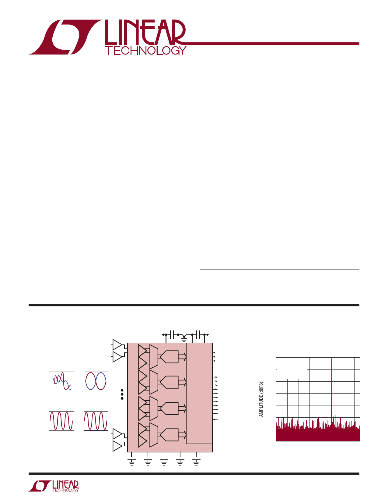
TYPICAL APPLICATION
3.3V OR 5V
10µF
1µF
1.8V TO 2.5V
TRUE DIFFERENTIAL INPUTS
NO CONFIGURATION REQUIRED
IN+, IN–
ARBITRARY
VDD
DIFFERENTIAL
VDD
0V 0V
BIPOLAR
VDD
UNIPOLAR
VDD
0V 0V
EIGHT SIMULTANEOUS
SAMPLING CHANNELS
AAIINN11+– S/H
AAIINN22+– S/H
MUX
VDD GND
14-BIT
+ SIGN
SAR ADC
GND OVDD
CMOS/LVDS
SDR/DDR
REFBUFEN
AAIINN33+– S/H
AAIINN44+– S/H
AAIINN55+– S/H
AAIINN66–+ S/H
14-BIT
MUX + SIGN
SAR ADC
LTC2320-14
14-BIT
MUX + SIGN
SAR ADC
SDO1
SDO2
SDO3
SDO4
SDO5
SDO6
SDO7
SDO8
CLKOUT
SCK
CNV
AAIINN77+– S/H
AAIINN88+– S/H
MUX
14-BIT
+ SIGN
SAR ADC
REF REFOUT1 REFOUT2 REFOUT3 REFOUT4
232014 TA01a
1µF 10µF 10µF 10µF 10µF
SAMPLE
CLOCK
For more information www.linear.com/LTC2320-14
32k
Point
FFT
fIN =
fS5SM0MP0PLkLH=z
1.5Msps,
IN
0 SNR = 81.1dB
–20
THD = –90.2dB
SINAD = 80.8dB
SFDR = 94.7dB
–40
–60
–80
–100
–120
–140
0
0.1 0.2 0.3 0.4 0.5 0.6 0.7
FREQUENCY (MHz)
232014 TA01b
232014f
1
1 page 
LTC2320-14
D IGITAL INPUTS AND DIGITAL OUTPUTS The l denotes the specifications which apply over the
full operating temperature range, otherwise specifications are at TA = 25°C (Note 4).
SYMBOL PARAMETER
CMOS Digital Inputs and Outputs
VIH High Level Input Voltage
VIL Low Level Input Voltage
IIN Digital Input Current
CIN Digital Input Capacitance
VOH High Level Output Voltage
VOL Low Level Output Voltage
IOZ Hi-Z Output Leakage Current
ISOURCE Output Source Current
ISINK Output Sink Current
LVDS Digital Inputs and Outputs
VID LVDS Differential Input Voltage
VIS LVDS Common Mode Input Voltage
VOD LVDS Differential Output Voltage
VOS LVDS Common Mode Output Voltage
VOD_LP Low Power LVDS Differential Output Voltage
VOS_LP Low Power LVDS Common Mode Output Voltage
CONDITIONS
CMOS/LVDS = GND
VIN = 0V to OVDD
IO = –500μA
IO = 500μA
VOUT = 0V to OVDD
VOUT = 0V
VOUT = OVDD
CMOS/LVDS = OVDD
100Ω Differential Termination
OVDD = 2.5V
100Ω Differential Termination
OVDD = 2.5V
100Ω Differential Termination
OVDD = 2.5V
100Ω Differential Termination
OVDD = 2.5V
100Ω Differential Termination
OVDD = 2.5V
100Ω Differential Termination
OVDD = 2.5V
MIN TYP MAX UNITS
l 0.8 • OVDD
l
l –10
l
l OVDD – 0.2
l
l –10
l
l
0.2 • OVDD
10
5
0.2
10
–10
10
V
V
μA
pF
V
V
μA
mA
mA
l 240
l1
l 220
l 0.85
l 100
l 0.85
600
1.45
350 600
1.2 1.4
200 350
1.2 1.4
mV
V
mV
V
mV
V
For more information www.linear.com/LTC2320-14
232014f
5
5 Page 
LTC2320-14
PIN FUNCTIONS
Pins that are the same for all digital I/O modes.
AFuINll6-+s,caAleIN6r–an(gPein(sA2IN,61+):–
Analog
AIN6–)
Differential Input Pins.
is ±REFOUT3 voltage.
These pins can be driven from VDD to GND.
GND (Pins 3, 7, 12, 18, 26, 32, 38, 46, 49): Ground.
These pins and exposed pad (Pin 53) must be tied directly
to a solid ground plane.
FAuINll5-+s,caAleIN5r–an(gPein(sA5IN,54+):–
Analog
AIN5–)
Differential Input Pins.
is ±REFOUT3 voltage.
These pins can be driven from VDD to GND.
REFOUT3 (Pin 6): Reference Buffer 3 Output. An onboard
buffer nominally outputs 4.096V to this pin. This pin is
referred to GND and should be decoupled closely to the
pin with a 10µF (X5R, 0805 size) ceramic capacitor. The
internal buffer driving this pin may be disabled by ground-
ing the REFBUFEN pin. If the buffer is disabled, an external
reference may drive this pin in the range of 1.25V to 5V.
REF (Pin 8): Common 4.096V reference output. Decouple
to GND with a 1μF low ESR ceramic capacitor. May be
overdriven with a single external reference to establish a
common reference for ADC cores 1 through 4.
REFOUT2 (Pin 9): Reference Buffer 2 Output. An onboard
buffer nominally outputs 4.096V to this pin. This pin is
referred to GND and should be decoupled closely to the
pin with a 10µF (X5R, 0805 size) ceramic capacitor. The
internal buffer driving this pin may be disabled by ground-
ing the REFBUFEN pin. If the buffer is disabled, an external
reference may drive this pin in the range of 1.25V to 5V.
AFuINll4-+s,cAalIeN4r–a(nPgiens(A1I1N,41+0–):
Analog Differential Input Pins.
AIN4–) is ±REFOUT2 voltage.
These pins can be driven from VDD to GND.
FAuINll3-+s,cAalIeN3r–a(nPgiens(A1I4N,31+3–):
Analog Differential Input Pins.
AIN3–) is ±REFOUT2 voltage.
These pins can be driven from VDD to GND.
VDD (Pins 15, 21, 44, 52): Power Supply. Bypass VDD to
GND with a 10µF ceramic capacitor and a 0.1µF ceramic
capacitor close to the part. The VDD pins should be shorted
together and driven from the same supply.
FAuINll2-+s,cAalIeN2r–a(nPgiens(A1I7N,21+6–):
Analog Differential Input Pins.
AIN2–) is ±REFOUT1 voltage.
These pins can be driven from VDD to GND.
FAuINll1-+s,cAalIeN1r–a(nPgiens(A2I0N,11+9–):
Analog Differential Input Pins.
AIN1–) is ±REFOUT1 voltage.
These pins can be driven from VDD to GND.
REFOUT1 (Pin 22): Reference Buffer 1 Output. An onboard
buffer nominally outputs 4.096V to this pin. This pin is
referred to GND and should be decoupled closely to the
pin with a 10µF (X5R, 0805 size) ceramic capacitor. The
internal buffer driving this pin may be disabled by ground-
ing the REFBUFEN pin. If the buffer is disabled, an external
reference may drive this pin in the range of 1.25V to 5V.
SDR/DDR (Pin 23): Double Data Rate Input. Controls the
frequency of SCK and CLKOUT. Tie to GND for the falling
edge of SCK to shift each serial data output (Single Data
Rate, SDR). Tie to OVDD to shift serial data output on each
edge of SCK (Double Data Rate, DDR). CLKOUT will be a
delayed version of SCK for both pin states.
CNV (Pin 24): Convert Input. This pin, when high, defines
the acquisition phase. When this pin is driven low, the
conversion phase is initiated and output data is clocked
out. This input must be driven at OVDD levels with a low
jitter pulse. This pin is unaffected by the CMOS/LVDS pin.
CMOS/LVDS (Pin 25): I/O Mode Select. Ground this pin
to enable CMOS mode, tie to OVDD to enable LVDS mode.
Float this pin to enable low power LVDS mode.
OVDD (Pins 31, 37): I/O Interface Digital Power. The range
of OVDD is 1.71V to 2.63V. This supply is nominally set
to the same supply as the host interface (CMOS: 1.8V or
2.5V, LVDS: 2.5V). Bypass OVDD to GND (Pins 32 and 38)
with 0.1µF capacitors.
For more information www.linear.com/LTC2320-14
232014f
11
11 Page | ||
| Páginas | Total 30 Páginas | |
| PDF Descargar | [ Datasheet LTC2320-14.PDF ] | |
Hoja de datos destacado
| Número de pieza | Descripción | Fabricantes |
| LTC2320-12 | 1.5Msps/Ch Simultaneous Sampling ADC | Linear Technology |
| LTC2320-14 | 1.5Msps/Ch Simultaneous Sampling ADC | Linear Technology |
| LTC2320-16 | 1.5Msps/Ch Simultaneous Sampling ADC | Linear Technology |
| Número de pieza | Descripción | Fabricantes |
| SLA6805M | High Voltage 3 phase Motor Driver IC. |
Sanken |
| SDC1742 | 12- and 14-Bit Hybrid Synchro / Resolver-to-Digital Converters. |
Analog Devices |
|
DataSheet.es es una pagina web que funciona como un repositorio de manuales o hoja de datos de muchos de los productos más populares, |
| DataSheet.es | 2020 | Privacy Policy | Contacto | Buscar |