|
|
|
PDF LTC6432-15 Data sheet ( Hoja de datos )
| Número de pieza | LTC6432-15 | |
| Descripción | 100kHz to 1.4GHz Differential ADC Driver/IF Amplifier | |
| Fabricantes | Linear | |
| Logotipo | ||
Hay una vista previa y un enlace de descarga de LTC6432-15 (archivo pdf) en la parte inferior de esta página. Total 20 Páginas | ||
|
No Preview Available !
FEATURES
nn 100kHz to 1400MHz Bandwidth
nn 54.4dBm OIP3 at 1MHz into a 100Ω Diff Load
nn 48.0dBm OIP3 at 150MHz into a 100Ω Diff Load
nn Up to 15dBm Output Power
nn NF = 3.0dB at 240MHz
nn Low 1/f Noise Corner
nn User Defined Low Frequency
nn 15.2dB Fixed Power Gain
nn A-Grade 100% OIP3 Tested at 150MHz
nn 0.8 nV/√Hz Total Input Noise
nn >2.75VP-P Linear Output Swing
nn P1dB = 22.5dBm
nn Insensitive to VCC Variation
nn Input/Output Internally Matched to 100Ω Differential
nn Single 5V Supply
nn DC Power = 850mW
nn Unconditionally Stable
APPLICATIONS
nn Differential 1GHz Bandwidth ADC Driver
nn Wideband Test Instrument Amplifier
nn Differential IF Amplifier
nn 50Ω/75Ω Balanced IF Amplifier
LTC6432-15
100kHz to 1.4GHz
Differential ADC Driver/IF
Amplifier
DESCRIPTION
The LTC®6432-15 is an ultra-high dynamic range differen-
tial gain block amplifier designed to drive high resolution,
high speed ADCs. It offers a full GHz of data bandwidth for
complex spectrally efficient modulations schemes or where
resistance to blockers is critical. This unique device can
simultaneously achieve low noise, incomparable linearity
and flat gain over the 100kHz to 1GHz band.
Unlike wideband GaAs PHEMTs, MESFETs and GaN FETs,
this SiGe based amplifier exhibits low 1/f noise and can
be used down to 100kHz.
The LTC6432-15 is designed for ease of use requiring a
minimum of support components. Impedance matching,
temperature compensation and bias control are handled
internally to ensure consistent performance over environ-
mental changes.
All A-Grade LTC6432-15 devices are tested and guaran-
teed for OIP3 at 150MHz. The LTC6432-15 is housed in
a 4mm × 4mm, 24L, QFN package with an exposed pad
for thermal management and low inductance.
For a single-ended 50Ω IF Gain Block with similar perfor-
mance, see the related LTC6433-15.
L, LT, LTC, LTM, Linear Technology and the Linear logo are registered trademarks of Analog
Devices, Inc. All other trademarks are the property of their respective owners.
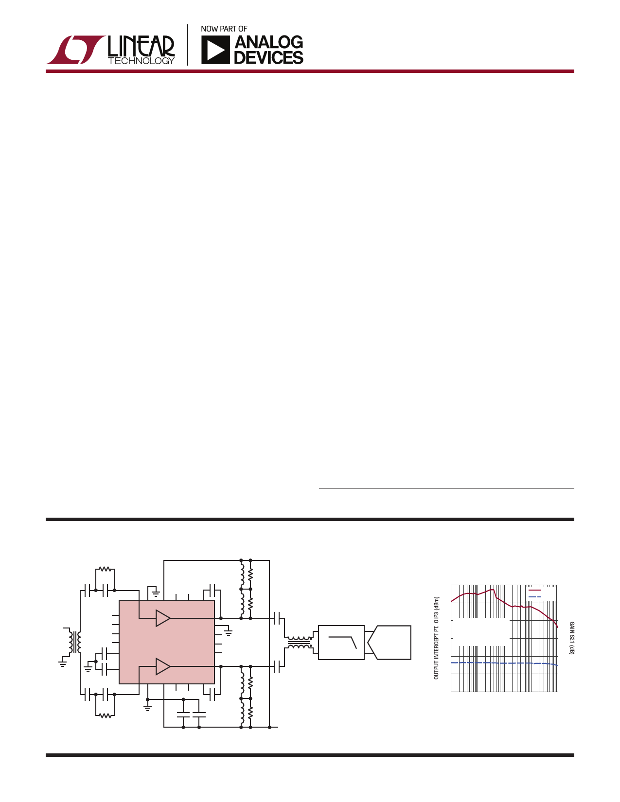
TYPICAL APPLICATION
350Ω
1µF 1µF
470µH
1µF
250Ω
INPUT •1:2•
+IN GND VCC DNC DNC +FDBK
DNC +OUT
240nH
DNC
DNC
1µF DNC
LTC6432-15
GND
DNC
T_DIODE
NFILT2
NFILT1
DNC
–OUT
1µF
–IN GND VCC DNC DNC –FDBK
240nH
280Ω 1µF
1:1
BALUN
1µF
+IN +OUT
LP FILTER
–IN –OUT
+IN
16-BIT ADC
–IN
280Ω
1µF 1µF
350Ω
1nF
643215 TA01a
1µF
1µF 470µH
250Ω
VCC = 5V
For more information www.linear.com/LTC6432-15
OIP3 and S21 vs Frequency
60 60
OIP3
S21
50 50
40 VCC = 5V
POUT = 4dBm/TONE
30
ZIN = ZOUT = 100Ω DIFF
TCASE = 30°C
20
40
30
20
10 10
00
0.1 1 10 100 1k
FREQUENCY (MHz)
643215 TA01b
643215f
1
1 page 
LTC6432-15
A C ELECTRICAL CHARACTERISTICS The l denotes the specifications which apply over the full operating
temperature range, otherwise
measurements are performed
specifications are at
using Test Circuit A,
mTCeAaSsEu=rin3g0°fCro(mNo5t0eΩ3)S.MVACCto=
550VΩ, ZSSMOUARCwEit=hoZuLOt AdDe-=em10b0eΩdd, iunngle(Nssotoeth4e)r.wise
noted,
SYMBOL PARAMETER
Frequency = 500MHz
S21 Differential Power Gain
OIP3 Output Third-Order Intercept Point
IM3 Third-Order Intermodulation
HD2 Second Harmonic Distortion
HD3 Third Harmonic Distortion
P1dB Output 1dB Compression Point
NF Noise Figure
Frequency = 1000MHz
S21 Differential Power Gain
OIP3 Output Third-Order Intercept Point
IM3 Third-Order Intermodulation
HD2
HD3
P1dB
NF
Second Harmonic Distortion
Third Harmonic Distortion
Output 1dB Compression Point
Noise Figure
CONDITIONS
De-Embedded to Package w Ext. 1µF FDBK Capacitor
POUT = 2dBm/Tone, ∆f = 1MHz, ZO = 100Ω Grade A
Grade B
P OUT = 2dBm/Tone, ∆f = 1MHz, ZO = 100Ω
Grade A
Grade B
POUT = 8dBm
POUT = 8dBm
De-Embedded to Package for Balun Input Loss
De-Embedded to Package w Ext. 1µF FDBK Capacitor
POUT = 2dBm/Tone, ∆f = 1MHz, ZO = 100Ω
Grade A
Grade B
P OUT = 2dBm/Tone, ∆f = 1MHz, ZO = 100Ω
Grade A
Grade B
POUT = 8dBm
POUT = 8dBm
De-Embedded to Package for Balun Input Loss
MIN TYP MAX UNITS
15.4
41
39
–78
–74
–82.9
–67.4
21.9
3.9
dB
dBm
dBm
dBc
dBc
dBc
dBc
dBm
dB
14.6
36
33
–68
–62
–67.2
–57.5
19.2
4.8
dB
dBm
dBm
dBc
dBc
dBc
dBc
dBm
dB
Note 1: Stresses beyond those listed under Absolute Maximum Ratings
may cause permanent damage to the device. Exposure to any Absolute
Maximum Rating condition for extended periods may affect device
reliability and lifetime.
Note 2: Guaranteed by design and characterization. This parameter is not
tested.
Note 3: The LTC6432-15 is guaranteed functional over the case operating
temperature range of –40 C to 85°C.
Note 4: Small signal parameters S and Noise are de-embedded to the
package pins, while large signal parameters are measured directly from
the test circuit.
For more information www.linear.com/LTC6432-15
643215f
5
5 Page 
LTC6432-15
OPERATION
The LTC6432-15 is a highly linear, fixed gain differential
amplifier. It can be considered a pair of 50Ω single-ended
devices operating 180 degrees apart. Its core signal path
consists of a single amplifier stage minimizing stability
issues. The input is a Darlington pair for high input imped-
ance and high current gain. Additional circuit enhance-
ments increase the output impedance commensurate with
the input impedance and minimize the effects of internal
Miller capacitance.
The LTC6432-15 uses a classic RF gain block topology,
with enhancements to achieve excellent linearity. Shunt
and Series feedback elements are added to simultane-
ously lower the input/output impedance and match them
to the 100Ω differential source and load. An internal bias
controller optimizes the bias point for peak linearity over
environmental changes. This circuit architecture provides
low noise, good RF power handling capability and wide
bandwidth; characteristics that are desirable for IF signal
chain applications.
APPLICATIONS INFORMATION
The LTC6432-15 is a highly linear fixed gain amplifier
designed for ease of use. Both the input and output are
matched to 100Ω differential source and load impedance
from 100kHz to 1000MHz using the specified evaluation
circuit. Biasing and temperature compensation are also
handled internally to deliver optimized performance. The
designer need only supply input/output blocking caps, RF
chokes, feedback caps, filter caps and decoupling caps
for the 5V supply. However, because the device is capable
of such wide band operation, a single application circuit
will probably not result in optimized performance across
the full frequency band.
Differential circuits minimize the common mode noise and
2nd harmonic distortion issues that plague many designs.
The LTC6432’s differential topology matches well with the
differential inputs of an ADC. However, evaluation of these
differential circuits is difficult, as high resolution, high
frequency, differential test equipment is lacking.
Our test circuit is designed for evaluation with standard
single-ended 50Ω test equipment. Therefore, 1:2 balun
transformers have been added to the input and output to
transform the LTC6432-15’s 100Ω differential source/load
impedance to 50Ω single-ended impedance, compatible
with most test equipment.
Other than the balun, the evaluation circuit requires a
minimum of external components. Input and output DC
blocking caps are required as this device is internally biased
for optimal operation. A frequency appropriate choke and
decoupling caps provide DC bias to the RF ±OUT nodes.
Only a single 5V supply is necessary to either of the VCC
pins on the device. Both VCC pins are connected inside
the package. Two VCC pins are provided for the conve-
nience of supply routing on the PCB. An optional parallel
1µF, 350Ω input network has been added to ensure low
frequency stability.
The particular element values shown in Test Circuit A are
chosen for wide bandwidth operation. Depending on the
desired frequency, performance may be improved by proper
selection of these supporting components.
Choosing the Right RF Choke
Not all choke inductors are created equal. It is always
important to select an inductor with low RLOSS as this will
drop the available voltage to the device. Also look for an
inductor with high self resonant frequency (SRF) as this
will limit the upper frequency where the choke is useful.
Above the SRF, the parasitic capacitance dominates and
the choke’s impedance will drop. For these reasons, wire
wound inductors are preferred, while multilayer ceramic
chip inductors should be avoided for an RF choke if pos-
sible. Since the LTC6432-15 is capable of such wideband
operation, a single choke value will not result in optimized
performance across its full frequency band. Table 1 list
common frequency bands and suggested corresponding
inductor values
For more information www.linear.com/LTC6432-15
643215f
11
11 Page | ||
| Páginas | Total 20 Páginas | |
| PDF Descargar | [ Datasheet LTC6432-15.PDF ] | |
Hoja de datos destacado
| Número de pieza | Descripción | Fabricantes |
| LTC6432-15 | 100kHz to 1.4GHz Differential ADC Driver/IF Amplifier | Linear |
| Número de pieza | Descripción | Fabricantes |
| SLA6805M | High Voltage 3 phase Motor Driver IC. |
Sanken |
| SDC1742 | 12- and 14-Bit Hybrid Synchro / Resolver-to-Digital Converters. |
Analog Devices |
|
DataSheet.es es una pagina web que funciona como un repositorio de manuales o hoja de datos de muchos de los productos más populares, |
| DataSheet.es | 2020 | Privacy Policy | Contacto | Buscar |