|
|
PDF MT8HTF3264HDY Data sheet ( Hoja de datos )
| Número de pieza | MT8HTF3264HDY | |
| Descripción | 256MB DDR2 SDRAM SODIMM | |
| Fabricantes | Micron | |
| Logotipo |  |
|
Hay una vista previa y un enlace de descarga de MT8HTF3264HDY (archivo pdf) en la parte inferior de esta página. Total 19 Páginas | ||
|
No Preview Available !
256MB, 512MB, 1GB (x64, DR) 200-Pin DDR2 SODIMM
Features
DDR2 SDRAM SODIMM
MT8HTF3264HDY – 256MB
MT8HTF6464HDY – 512MB
MT8HTF12864HDY – 1GB
Features
• 200-pin, small-outline dual in-line memory module
(SODIMM)
• Fast data transfer rates: PC2-3200, PC2-4200,
PC2-5300, or PC2-6400
• 256MB (32 Meg x 64), 512MB (64 Meg x 64), or 1GB
(128 Meg x 64)
• VDD = 1.8V
• VDDSPD = 1.7–3.6V
• JEDEC-standard 1.8V I/O (SSTL_18-compatible)
• Differential data strobe (DQS, DQS#) option
• 4n-bit prefetch architecture
• Multiple internal device banks for concurrent opera-
tion
• Programmable CAS latency (CL)
• Posted CAS additive latency (AL)
• WRITE latency = READ latency - 1 tCK
• Programmable burst lengths (BL): 4 or 8
• Adjustable data-output drive strength
• 64ms, 8192-cycle refresh
• On-die termination (ODT)
• Serial presence detect (SPD) with EEPROM
• Gold edge contacts
• Dual rank
Figure 1: 200-Pin SODIMM (MO-224 R/C A)
Module height: 30mm (1.18in)
Options
• Operating temperature
– Commercial (0°C ≤ TA ≤ +70°C)
– Industrial (–40°C ≤ TA ≤ +85°C)1
• Package
– 200-pin DIMM (lead-free)
• Frequency/CL2
– 2.5ns @ CL = 5 (DDR2-800)
– 2.5ns @ CL = 6 (DDR2-800)
– 3.0ns @ CL = 5 (DDR2-667)
– 3.75ns @ CL = 4 (DDR2-553)3
– 5.0ns @ CL = 3 (DDR2-400)3
Marking
D
T
Y
-80E
-800
-667
-53E
-40E
Notes:
1. Contact Micron for industrial temperature
module offerings.
2. CL = CAS (READ) latency.
3. Not recommended for new designs.
Table 1: Key Timing Parameters
Speed
Grade
-80E
-800
-667
-53E
-40E
Industry
Nomenclature
PC2-6400
PC2-6400
PC2-5300
PC2-4200
PC2-3200
CL = 6
800
800
–
–
–
Data Rate (MT/s)
CL = 5
CL = 4
800 533
667 533
667 553
– 553
– 400
CL = 3
400
400
400
400
400
tRCD
(ns)
12.5
15
15
15
15
tRP
(ns)
12.5
15
15
15
15
tRC
(ns)
55
55
55
55
55
PDF: 09005aef80ebed66
htf8c32_64_128x64hd.pdf - Rev. E 3/10 EN
1 Micron Technology, Inc. reserves the right to change products or specifications without notice.
© 2006 Micron Technology, Inc. All rights reserved.
Products and specifications discussed herein are subject to change by Micron without notice.
1 page 
256MB, 512MB, 1GB (x64, DR) 200-Pin DDR2 SODIMM
Pin Descriptions
Pin Descriptions
The pin description table below is a comprehensive list of all possible pins for all DDR2
modules. All pins listed may not be supported on this module. See Pin Assignments for
information specific to this module.
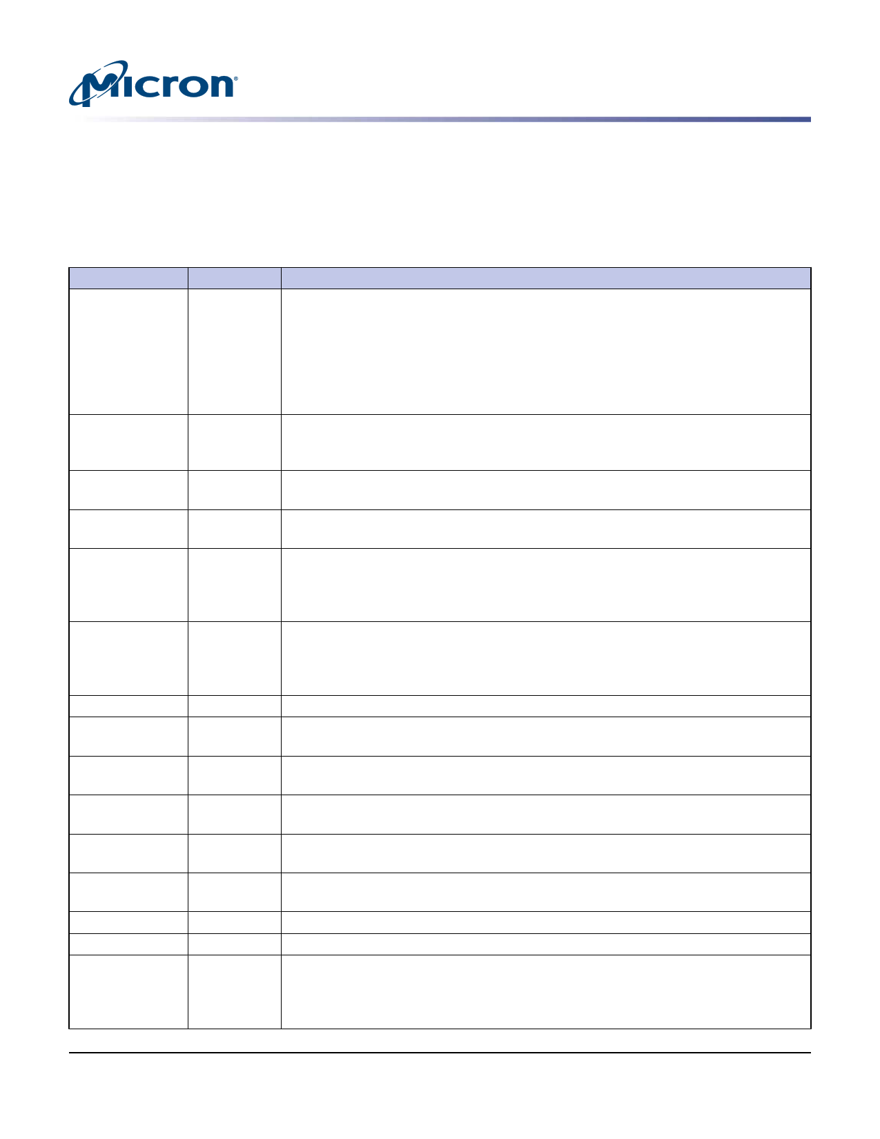
Table 7: Pin Descriptions
Symbol
Ax
Type
Input
BAx
CKx,
CK#x
CKEx
DMx,
Input
Input
Input
Input
ODTx
Input
Par_In
RAS#, CAS#, WE#
RESET#
S#x
SAx
SCL
CBx
DQx
DQSx,
DQS#x
Input
Input
Input
Input
Input
Input
I/O
I/O
I/O
Description
Address inputs: Provide the row address for ACTIVE commands, and the column ad-
dress and auto precharge bit (A10) for READ/WRITE commands, to select one location
out of the memory array in the respective bank. A10 sampled during a PRECHARGE
command determines whether the PRECHARGE applies to one bank (A10 LOW, bank
selected by BAx) or all banks (A10 HIGH). The address inputs also provide the op-code
during a LOAD MODE command. See the Pin Assignments Table for density-specific
addressing information.
Bank address inputs: Define the device bank to which an ACTIVE, READ, WRITE, or
PRECHARGE command is being applied. BA define which mode register (MR0, MR1,
MR2, and MR3) is loaded during the LOAD MODE command.
Clock: Differential clock inputs. All control, command, and address input signals are
sampled on the crossing of the positive edge of CK and the negative edge of CK#.
Clock enable: Enables (registered HIGH) and disables (registered LOW) internal circui-
try and clocks on the DDR2 SDRAM.
Data mask (x8 devices only): DM is an input mask signal for write data. Input data
is masked when DM is sampled HIGH, along with that input data, during a write ac-
cess. Although DM pins are input-only, DM loading is designed to match that of the
DQ and DQS pins.
On-die termination: Enables (registered HIGH) and disables (registered LOW) termi-
nation resistance internal to the DDR2 SDRAM. When enabled in normal operation,
ODT is only applied to the following pins: DQ, DQS, DQS#, DM, and CB. The ODT input
will be ignored if disabled via the LOAD MODE command.
Parity input: Parity bit for Ax, RAS#, CAS#, and WE#.
Command inputs: RAS#, CAS#, and WE# (along with S#) define the command being
entered.
Reset: Asynchronously forces all registered outputs LOW when RESET# is LOW. This
signal can be used during power-up to ensure that CKE is LOW and DQ are High-Z.
Chip select: Enables (registered LOW) and disables (registered HIGH) the command
decoder.
Serial address inputs: Used to configure the SPD EEPROM address range on the I2C
bus.
Serial clock for SPD EEPROM: Used to synchronize communication to and from the
SPD EEPROM on the I2C bus.
Check bits. Used for system error detection and correction.
Data input/output: Bidirectional data bus.
Data strobe: Travels with the DQ and is used to capture DQ at the DRAM or the con-
troller. Output with read data; input with write data for source synchronous opera-
tion. DQS# is only used when differential data strobe mode is enabled via the LOAD
MODE command.
PDF: 09005aef80ebed66
htf8c32_64_128x64hd.pdf - Rev. E 3/10 EN
5 Micron Technology, Inc. reserves the right to change products or specifications without notice.
© 2006 Micron Technology, Inc. All rights reserved.
5 Page 
IDD Specifications
256MB, 512MB, 1GB (x64, DR) 200-Pin DDR2 SODIMM
IDD Specifications
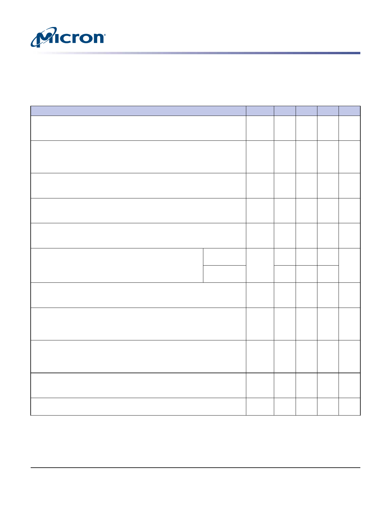
Table 10: DDR2 IDD Specifications and Conditions – 256MB
Values shown for MT47H16M16 DDR2 SDRAM only and are computed from values specified in the 256Mb (16 Meg x 16)
component data sheet
Parameter
Symbol -667 -53E -40E Units
Operating one bank active-precharge current:tCK = tCK (IDD), tRC = tRC
(IDD), tRAS = tRAS MIN (IDD); CKE is HIGH, S# is HIGH between valid commands;
Address bus inputs are switching; Data bus inputs are switching
IDD01
380 340 320 mA
Operating one bank active-read-precharge current: IOUT = 0mA; BL = 4, CL
= CL (IDD), AL = 0; tCK = tCK (IDD), tRC = tRC (IDD), tRAS = tRAS MIN (IDD), tRCD =
tRCD (IDD); CKE is HIGH, S# is HIGH between valid commands; Address bus in-
puts are switching; Data pattern is same as IDD4W
IDD11
420 380 360 mA
Precharge power-down current: All device banks idle; tCK = tCK (IDD); CKE is IDD2P2 40 40 40 mA
LOW; Other control and address bus inputs are stable; Data bus inputs are float-
ing
Precharge quiet standby current: All device banks idle; tCK = tCK (IDD); CKE IDD2Q2 400 280 200 mA
is HIGH, S# is HIGH; Other control and address bus inputs are stable; Data bus
inputs are floating
Precharge standby current: All device banks idle; tCK = tCK (IDD); CKE is
IDD2N2 320 280 240 mA
HIGH, S# is HIGH; Other control and address bus inputs are switching; Data bus
inputs are switching
Active power-down current: All device banks open; tCK = Fast PDN exit IDD3P2 240 200 160 mA
tCK (IDD); CKE is LOW; Other control and address bus inputs are MR[12] = 0
stable; Data bus inputs are floating
Slow PDN exit
48 48 48
MR[12] = 1
Active standby current: All device banks open; tCK = tCK (IDD), tRAS = tRAS
IDD3N2 440 320 240 mA
MAX (IDD), tRP = tRP (IDD); CKE is HIGH, S# is HIGH between valid commands;
Other control and address bus inputs are switching; Data bus inputs are switching
Operating burst write current: All device banks open; Continuous burst
IDD4W1 880 740 580 mA
writes; BL = 4, CL = CL (IDD), AL = 0; tCK = tCK (IDD), tRAS = tRAS MAX (IDD), tRP =
tRP (IDD); CKE is HIGH, S# is HIGH between valid commands; Address bus inputs
are switching; Data bus inputs are switching
Operating burst read current: All device banks open; Continuous burst read, IDD4R1 780 660 500 mA
IOUT = 0mA; BL = 4, CL = CL (IDD), AL = 0; tCK = tCK (IDD), tRAS = tRAS MAX (IDD),
tRP = tRP (IDD); CKE is HIGH, S# is HIGH between valid commands; Address bus
inputs are switching; Data bus inputs are switching
Burst refresh current:tCK = tCK (IDD); REFRESH command at every tRFC (IDD)
interval; CKE is HIGH, S# is HIGH between valid commands; Other control and
address bus inputs are switching; Data bus inputs are switching
IDD52 1440 1360 1320 mA
Self refresh current: CK and CK# at 0V; CKE ≤ 0.2V; Other control and ad-
dress bus inputs are floating; Data bus inputs are floating
IDD62 40 40 40 mA
PDF: 09005aef80ebed66
htf8c32_64_128x64hd.pdf - Rev. E 3/10 EN
11
Micron Technology, Inc. reserves the right to change products or specifications without notice.
© 2006 Micron Technology, Inc. All rights reserved.
11 Page | ||
| Páginas | Total 19 Páginas | |
| PDF Descargar | [ Datasheet MT8HTF3264HDY.PDF ] | |
Hoja de datos destacado
| Número de pieza | Descripción | Fabricantes |
| MT8HTF3264HDY | 256MB DDR2 SDRAM SODIMM | Micron |
| Número de pieza | Descripción | Fabricantes |
| SLA6805M | High Voltage 3 phase Motor Driver IC. |
Sanken |
| SDC1742 | 12- and 14-Bit Hybrid Synchro / Resolver-to-Digital Converters. |
Analog Devices |
|
DataSheet.es es una pagina web que funciona como un repositorio de manuales o hoja de datos de muchos de los productos más populares, |
| DataSheet.es | 2020 | Privacy Policy | Contacto | Buscar |
