|
|
|
PDF MT36VDDT51272 Data sheet ( Hoja de datos )
| Número de pieza | MT36VDDT51272 | |
| Descripción | 4GB DDR SDRAM RDIMM | |
| Fabricantes | Micron | |
| Logotipo | ||
Hay una vista previa y un enlace de descarga de MT36VDDT51272 (archivo pdf) en la parte inferior de esta página. Total 18 Páginas | ||
|
No Preview Available !
1GB, 2GB, 4GB (x72, ECC, DR) 184-Pin DDR RDIMM
Features
DDR SDRAM RDIMM
MT36VDDT12872 – 1GB1
MT36VDDT25672 – 2GB1
MT36VDDT51272 – 4GB
For component data sheets, refer to Micron’s Web site: www.micron.com
Features
• 184-pin, registered dual in-line memory module
(RDIMM)
• Standard and low profile height PCB modules
• Fast data transfer rates: PC2100 or PC2700
• 1GB (128 Meg x 72), 2GB (256 Meg x 72),
and 4GB (512 Meg x 72)
• Supports ECC error detection and correction
• VDD = VDDQ = +2.5V
• VDDSPD = +2.3V to +3.6V
• 2.5V I/O (SSTL_2-compatible)
• Internal, pipelined double data rate (DDR)
2n-prefetch architecture
• Bidirectional data strobe (DQS) transmitted/
received with data—that is, source-synchronous
data capture
• Differential clock inputs (CK and CK#)
• Multiple internal device banks for concurrent
operation
• Dual rank
• Selectable burst lengths (BL): 2, 4, or 8
• Auto precharge option
• Auto refresh and self refresh modes: 7.8125µs
maximum average periodic refresh interval
• Serial presence-detect (SPD) with EEPROM
• Selectable CAS latency (CL) for maximum
compatibility
• Gold edge contacts
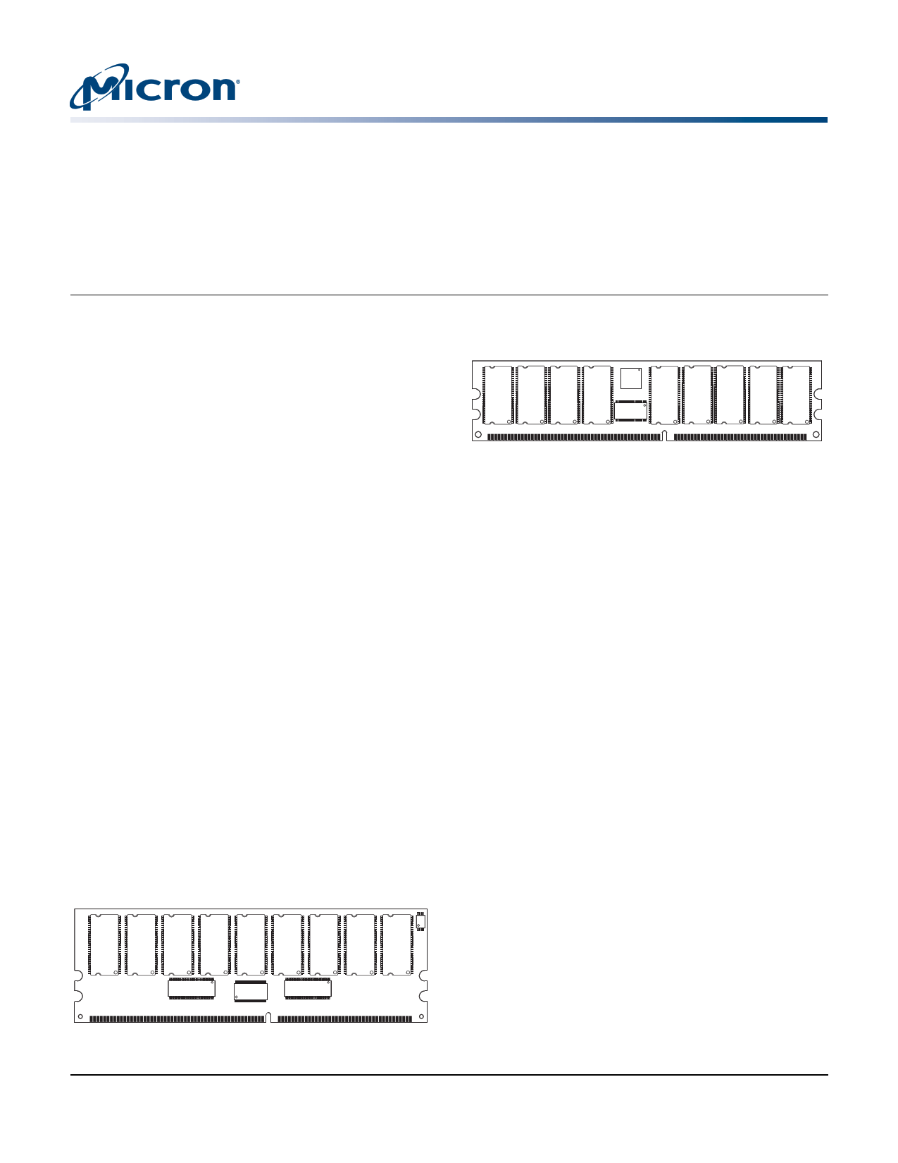
184-Pin RDIMM Figures
Figure 1: Standard-Height Layout (MO-206)
PCB height: 43.18mm (1.7in)
Figure 2: Low-Profile Layout (MO-206)
PCB height: 30.48mm (1.2in)
Options
Marking
• Operating temperature2
– Commercial (0°C ≤ TA ≤ +70°C)
– Industrial (–40°C ≤ TA ≤ +85°C)
• Package
None
I
– 184-pin DIMM (standard)
G
– 184-pin DIMM (Pb-free)
• Memory clock, speed, CAS latency3
Y
– 6.0ns (167 MHz), 333 MT/s, CL = 2.5
– 7.5ns (133 MHz), 266 MT/s, CL = 24
– 7.5ns (133 MHz), 266 MT/s, CL = 24
-335
-262
-26A
– 7.5ns (133 MHz), 266 MT/s, CL = 2
-265
Notes: 1. End of life.
2. Contact Micron for industrial temperature
module offerings.
3. CL = CAS (READ) latency; registered mode
will add one clock cycle to CL.
4. Not recommended for new designs.
PDF: 09005aef809d5451/Source: 09005aef807da325
dd36c128_256_512x72.fm - Rev. F 6/08 EN
1 Micron Technology, Inc., reserves the right to change products or specifications without notice.
©2003 Micron Technology, Inc. All rights reserved.
Products and specifications discussed herein are subject to change by Micron without notice.
1 page 
1GB, 2GB, 4GB (x72, ECC, DR) 184-Pin DDR RDIMM
Pin Assignments and Descriptions
Table 7: Pin Descriptions
Symbol
A0–A13
BA0, BA1
CK0, CK0#
CKE0, CKE1
RAS#, CAS#, WE#
RESET#
S0#, S1#
SA0–SA2
SCL
CB0–CB7
DQ0–DQ63
DQS0–DQS17
SDA
VDD/VDDQ
VDDSPD
VREF
VSS
NC
NF
Type
Input
Input
Input
Input
Input
Input
Input
Input
Input
I/O
I/O
I/O
I/O
Supply
Supply
Supply
Supply
–
–
Description
Address inputs: Provide the row address for ACTIVE commands, and the
column address and auto precharge bit (A10) for READ/WRITE commands, to
select one location out of the memory array in the respective device bank. A10
sampled during a PRECHARGE command determines whether the PRECHARGE
applies to one device bank (A10 LOW, device bank selected by BA0 and BA1)
or all device banks (A10 HIGH). The address inputs also provide the op-code
during a MODE REGISTER SET command. BA0 and BA1 define which mode
register (mode register or extended mode register) is loaded during the LOAD
MODE REGISTER command. A0–A12 (1GB, 2GB ) or A0–A13 (4GB).
Bank address: BA0 and BA1 define the device bank to which an ACTIVE,
READ, WRITE, or PRECHARGE command is being applied.
Clock: CK and CK# are differential clock inputs. All control, command, and
address input signals are sampled on the crossing of the positive edge of CK
and the negative edge of CK#. Output data (DQ and DQS) is referenced to the
crossings of CK and CK#.
Clock enable: CKE enables (registered HIGH) and CKE disables (registered
LOW) the internal clock, input buffers, and output drivers.
Command inputs: RAS#, CAS#, and WE# (along with S#) define the command
being entered.
Reset: Asynchronously forces all registered outputs LOW when RESET# is LOW.
This signal can be used during power-up to ensure that CKE is LOW and DQ are
High-Z.
Chip select: S# enables (registered LOW) and disables (registered HIGH) the
command decoder.
Presence-detect address inputs: These pins are used to configure the SPD
EEPROM address range on the I2C bus.
Serial clock for SPD EEPROM: SCL is used to synchronize the presence-detect
data transfer to and from the module.
Check bits.
Data input/output: Data bus.
Data strobe: Output with read data. Edge-aligned with read data. Input with
write data. Center-aligned with write data. Used to capture data.
Serial data: SDA is a bidirectional pin used to transfer addresses and data into
and out of the presence-detect portion of the module.
Power supply: +2.5V ±0.2V.
SPD EEPROM power supply: +2.3V to +3.6V.
SSTL_2 reference voltage (VDD/2).
Ground.
No connect: These pins are not connected on the module.
No function: These pins are connected within the module, but provide no
functionality.
PDF: 09005aef809d5451/Source: 09005aef807da325
dd36c128_256_512x72.fm - Rev. F 6/08 EN
5 Micron Technology, Inc., reserves the right to change products or specifications without notice.
©2003 Micron Technology, Inc. All rights reserved
5 Page 
1GB, 2GB, 4GB (x72, ECC, DR) 184-Pin DDR RDIMM
Electrical Specifications
IDD Specifications
Table 10:
IDD Specifications and Conditions – 1GB
Values are for the MT46V64M4 DDR SDRAM only and are computed from values specified in the
256Mb (64 Meg x 4) component data sheet
Parameter/Condition
Operating one bank active-precharge current: tRC = tRC (MIN);
tCK = tCK (MIN); DQ, DM, and DQS inputs changing once per clock cycle;
Address and control inputs changing once every two clock cycles
Operating one bank active-read-precharge current: BL = 2;
tRC = tRC (MIN); tCK = tCK (MIN); IOUT = 0mA; Address and control inputs
changing once per clock cycle
Precharge power-down standby current: All device banks idle; Power-
down mode; tCK = tCK (MIN); CKE = LOW
Idle standby current: CS# = HIGH; All device banks idle; tCK = tCK (MIN);
CKE = HIGH; Address and other control inputs changing once per clock cycle;
VIN = VREF for DQ, DM, and DQS
Active power-down standby current: One device bank active; Power-
down mode; tCK = tCK (MIN); CKE = LOW
Active standby current: CS# = HIGH; CKE = HIGH; One device bank active;
tRC = tRAS (MAX); tCK = tCK (MIN); DQ, DM, and DQS inputs changing twice
per clock cycle; Address and other control inputs changing once per clock
cycle
Operating burst read current: BL = 2; Continuous burst reads; One
device bank active; Address and control inputs changing once per clock
cycle; tCK = tCK (MIN); IOUT = 0mA
Operating burst write current: BL = 2; Continuous burst writes; One
device bank active; Address and control inputs changing once per clock
cycle; tCK = tCK (MIN); DQ, DM, and DQS inputs changing twice per clock
cycle
Auto refresh current
tREFC = tRFC (MIN)
tREFC = 15.625µs
Self refresh current: CKE ≤ 0.2V
Operating bank interleave read current: Four device bank interleaving
reads (BL = 4) with auto precharge; tRC = tRC (MIN); tCK = tCK (MIN);
Address and control inputs change only during active READ or WRITE
commands
Symbol
IDD01
IDD11
IDD2P2
IDD2F2
IDD3P2
IDD3N2
IDD4R2
IDD4W2
IDD52
IDD5A2
IDD62
IDD71
-335
2,322
3,132
144
1,800
1,080
2,160
3,222
3,222
9,180
216
144
7,452
-26A
2,232
2,682
144
1,620
900
1,800
2,772
2,772
8,460
216
144
6,372
-265 Units
2,232 mA
2,682 mA
144 mA
1,620 mA
1,080 mA
1,800 mA
2,772 mA
2,772 mA
8,820
216
144
6,642
mA
mA
mA
mA
Notes:
1. Value calculated as one module rank in this operating condition; all other module ranks in
IDD2P (CKE LOW) mode.
2. Value calculated reflects all module ranks in this operating condition.
PDF: 09005aef809d5451/Source: 09005aef807da325
dd36c128_256_512x72.fm - Rev. F 6/08 EN
11
Micron Technology, Inc., reserves the right to change products or specifications without notice.
©2003 Micron Technology, Inc. All rights reserved
11 Page | ||
| Páginas | Total 18 Páginas | |
| PDF Descargar | [ Datasheet MT36VDDT51272.PDF ] | |
Hoja de datos destacado
| Número de pieza | Descripción | Fabricantes |
| MT36VDDT51272 | 4GB DDR SDRAM RDIMM | Micron |
| Número de pieza | Descripción | Fabricantes |
| SLA6805M | High Voltage 3 phase Motor Driver IC. |
Sanken |
| SDC1742 | 12- and 14-Bit Hybrid Synchro / Resolver-to-Digital Converters. |
Analog Devices |
|
DataSheet.es es una pagina web que funciona como un repositorio de manuales o hoja de datos de muchos de los productos más populares, |
| DataSheet.es | 2020 | Privacy Policy | Contacto | Buscar |