|
|
|
PDF MC74HCT4052A Data sheet ( Hoja de datos )
| Número de pieza | MC74HCT4052A | |
| Descripción | Analog Multiplexers / Demultiplexers | |
| Fabricantes | ON Semiconductor | |
| Logotipo | ||
Hay una vista previa y un enlace de descarga de MC74HCT4052A (archivo pdf) en la parte inferior de esta página. Total 16 Páginas | ||
|
No Preview Available !
MC74HCT4051A,
MC74HCT4052A,
MC74HCT4053A
Analog Multiplexers /
Demultiplexers with LSTTL
Compatible Inputs
High−Performance Silicon−Gate CMOS
The MC74HCT4051A, MC74HCT4052A and MC74HCT4053A
utilize silicon−gate CMOS technology to achieve fast propagation
delays, low ON resistances, and low OFF leakage currents. These
analog multiplexers/demultiplexers control analog voltages that may
vary across the complete power supply range (from VCC to VEE).
The HCT4051A, HCT4052A and HCT4053A are identical in
pinout to the metal−gate MC14051AB, MC14052AB and
MC14053AB. The Channel−Select inputs determine which one of the
Analog Inputs/Outputs is to be connected, by means of an analog
switch, to the Common Output/Input. When the Enable pin is HIGH,
all analog switches are turned off.
The Channel−Select and Enable inputs are compatible with standard
CMOS and LSTTL outputs.
These devices have been designed so that the ON resistance (Ron) is
more linear over input voltage than Ron of metal−gate CMOS analog
switches.
For a multiplexer/demultiplexer with injection current protection,
see HC4851A and HCT4851A.
Features
• Fast Switching and Propagation Speeds
• Low Crosstalk Between Switches
• Diode Protection on All Inputs/Outputs
• Analog Power Supply Range (VCC − VEE) = 2.0 to 12.0 V
• Digital (Control) Power Supply Range (VCC − GND) = 2.0 to 6.0 V
• Improved Linearity and Lower ON Resistance Than Metal−Gate
Counterparts
• Low Noise
• In Compliance with the Requirements of JEDEC Standard No. 7 A
• Chip Complexity: HCT4051A − 184 FETs or 46 Equivalent Gates
HCT4052A − 168 FETs or 42 Equivalent Gates
HCT4053A − 156 FETs or 39 Equivalent Gates
• These Devices are Pb−Free and are RoHS Compliant
16
1
16
1
16
1
http://onsemi.com
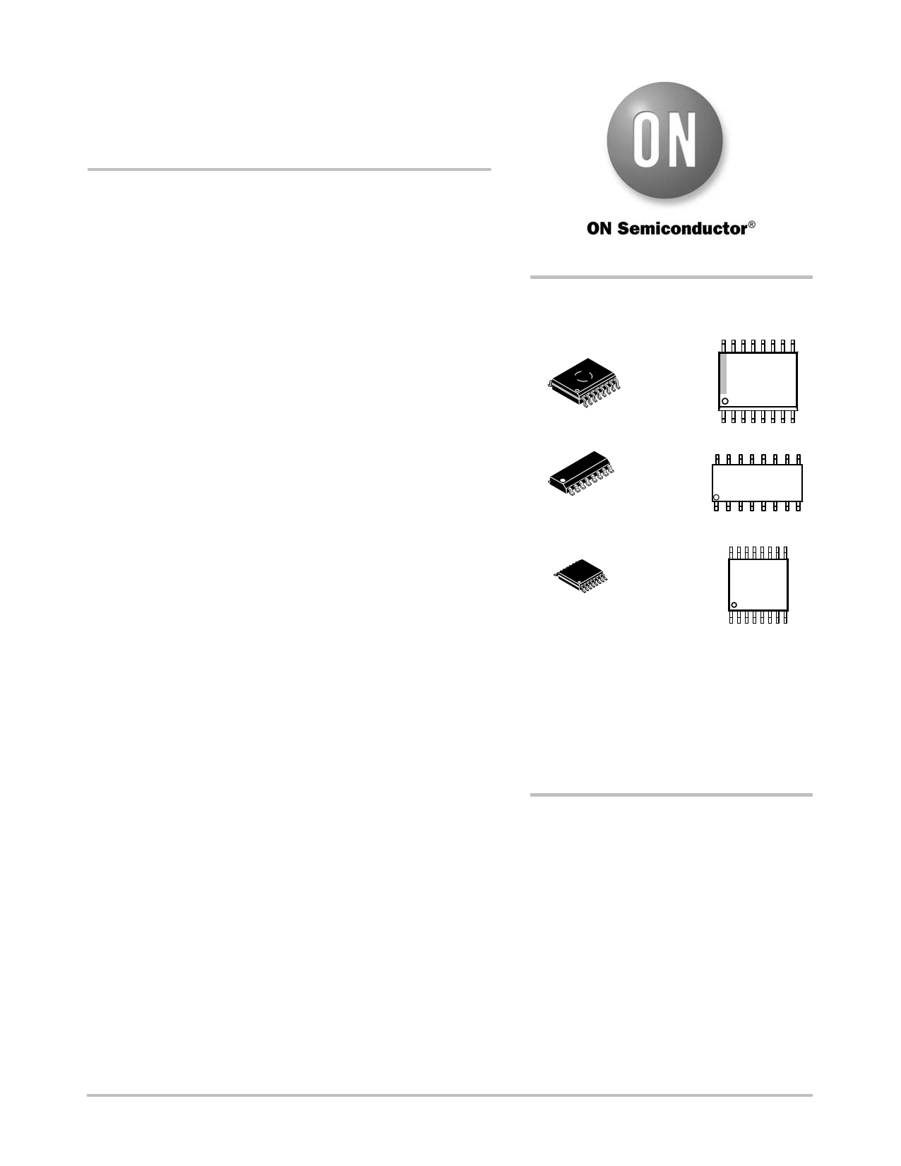
MARKING
DIAGRAMS
16
SOIC−16 WIDE
DW SUFFIX
CASE 751G
HCT405xA
AWLYWWG
1
16
SOIC−16
D SUFFIX
CASE 751B
HCT405xAG
AWLYWW
1
TSSOP−16
DT SUFFIX
CASE 948F
16
HCT40
5xA
ALYWG
G
1
x = 1, 2, 3
A = Assembly Location
WL, L = Wafer Lot
YY, Y = Year
WW, W = Work Week
G or G = Pb−Free Package
(Note: Microdot may be in either location)
ORDERING INFORMATION
See detailed ordering and shipping information in the package
dimensions section on page 13 of this data sheet.
© Semiconductor Components Industries, LLC, 2011
June, 2011 − Rev. 2
1
Publication Order Number:
MC74HCT4051A/D
1 page 
MC74HCT4051A, MC74HCT4052A, MC74HCT4053A
AC CHARACTERISTICS (CL = 50 pF, Input tr = tf = 6 ns)
Symbol
tPLH,
tPHL
Parameter
Maximum Propagation Delay, Channel−Select to Analog Output
(Figure 15)
tPLH,
tPHL
Maximum Propagation Delay, Analog Input to Analog Output
(Figure 16)
tPLZ,
tPHZ
Maximum Propagation Delay, Enable to Analog Output
(Figure 17)
tPZL,
tPZH
Maximum Propagation Delay, Enable to Analog Output
(Figure 17)
Cin Maximum Input Capacitance, Channel−Select or Enable Inputs
CI/O Maximum Capacitance
Analog I/O
(All Switches Off)
Common O/I: HCT4051A
HCT4052A
HCT4053A
Feed−through
VCC Guaranteed Limit
V −55 to 25°C ≤85°C ≤125°C Unit
2.0 270
3.0 90
4.5 59
6.0 45
320 350 ns
110 125
79 85
65 75
2.0 40
3.0 25
4.5 12
6.0 10
60 70 ns
30 32
15 18
13 15
2.0 160
3.0 70
4.5 48
6.0 39
200 220 ns
95 110
63 76
55 63
2.0 245
3.0 115
4.5 49
6.0 39
315 345 ns
145 155
69 83
58 67
10 10 10 pF
35 35 35 pF
130 130 130
80 80 80
50 50 50
1.0 1.0 1.0
Typical @ 25°C, VCC = 5.0 V, VEE = 0 V
CPD Power Dissipation Capacitance (Figure 19)*
HCT4051A
HCT4052A
HCT4053A
45
80
45
*Used to determine the no−load dynamic power consumption: PD = CPD VCC2f + ICC VCC.
pF
http://onsemi.com
5
5 Page 
MC74HCT4051A, MC74HCT4052A, MC74HCT4053A
+5V
+5V
ANALOG
16
ANALOG
+5V
ON
-5V SIGNAL
SIGNAL
-5V
6 11 TO EXTERNAL CMOS
7 10 CIRCUITRY 0 to 5V
8 9 DIGITAL SIGNALS
-5V
Figure 21. Application Example
VCC VCC VCC
Dx 16 Dx
ON/OFF
Dx Dx
VEE VEE
7
8
VEE
Figure 22. External Germanium or
Schottky Clipping Diodes
+5V
+5V
ANALOG
16
ANALOG
+5V
ON/OFF
VEE SIGNAL
SIGNAL
+5V
VEE
HC405x *
RRR
+5V
+5V
ANALOG
16
ANALOG
+5V
ON/OFF
VEE SIGNAL
SIGNAL
VEE
HCT405x
+5V
6 11
7 10
89
LSTTL/NMOS
CIRCUITRY
VEE * 2K ≤ R ≤ 10K
6 11
7 10
89
VEE
LSTTL/NMOS
CIRCUITRY
a. Using Pull−Up Resistors with a HC Device
b. Using HCT Interface
Figure 23. Interfacing LSTTL/NMOS to CMOS Inputs
11
A
LEVEL
SHIFTER
13
X0
14
X1
10
B
LEVEL
SHIFTER
15
X2
12
X3
9
C
LEVEL
SHIFTER
1
X4
5
X5
6
ENABLE
LEVEL
SHIFTER
2
X6
4
X7
Figure 24. Function Diagram, HCT4051A
3
X
http://onsemi.com
11
11 Page | ||
| Páginas | Total 16 Páginas | |
| PDF Descargar | [ Datasheet MC74HCT4052A.PDF ] | |
Hoja de datos destacado
| Número de pieza | Descripción | Fabricantes |
| MC74HCT4052A | Analog Multiplexers / Demultiplexers | ON Semiconductor |
| MC74HCT4052A | Analog Multiplexers / Demultiplexers | ON Semiconductor |
| Número de pieza | Descripción | Fabricantes |
| SLA6805M | High Voltage 3 phase Motor Driver IC. |
Sanken |
| SDC1742 | 12- and 14-Bit Hybrid Synchro / Resolver-to-Digital Converters. |
Analog Devices |
|
DataSheet.es es una pagina web que funciona como un repositorio de manuales o hoja de datos de muchos de los productos más populares, |
| DataSheet.es | 2020 | Privacy Policy | Contacto | Buscar |