|
|
|
PDF M5M42S6S-12 Data sheet ( Hoja de datos )
| Número de pieza | M5M42S6S-12 | |
| Descripción | 256K-Bit DRAM | |
| Fabricantes | Mitsubishi | |
| Logotipo | ||
Hay una vista previa y un enlace de descarga de M5M42S6S-12 (archivo pdf) en la parte inferior de esta página. Total 15 Páginas | ||
|
No Preview Available !
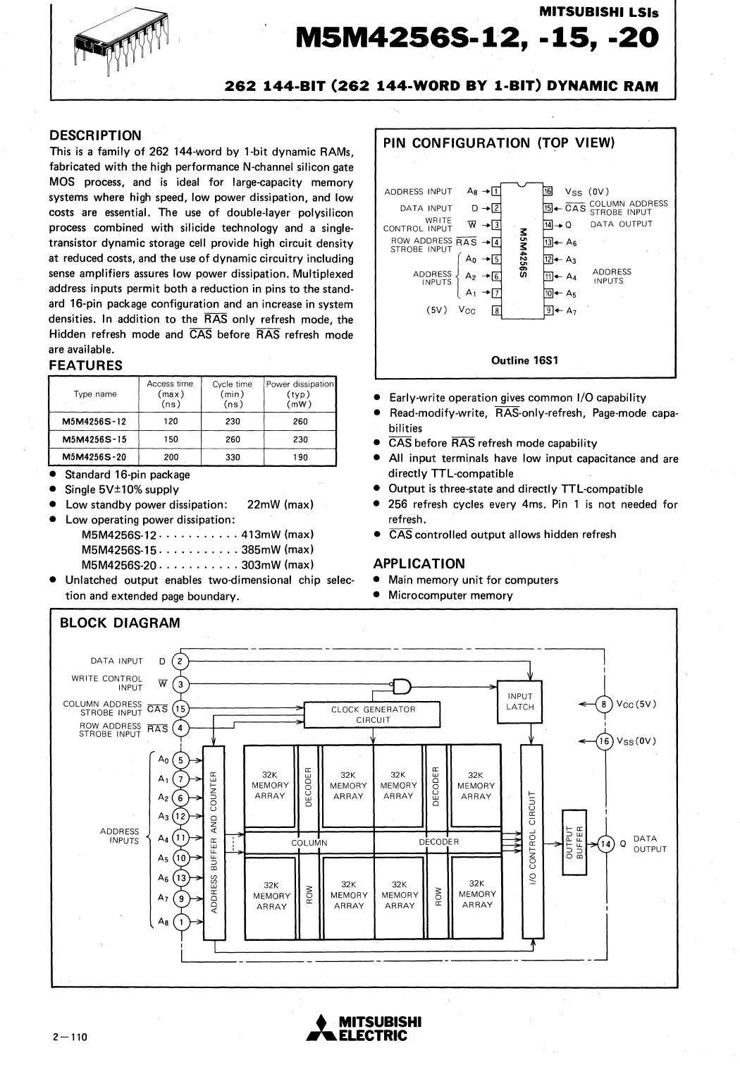
MITSUBISHI LSls
MSM42S6S-12, -15, -20
262 144-BIT (262 144-WORD BY 1-BIT) DYNAMIC RAM
DESCRIPTION
This is a family of 262 144-word by 1-bit dynamic RAMs,
fabricated with the high performance N-channel silicon gate
MOS process, and is ideal for large-capacity memory
systems where high speed, lOiN power dissipation, and low
costs are essential. The use of double-layer polysilicon
process combined with silicide technology and a single-
transistor dynamic storage cell provide high circuit density
at reduced costs, and the use of dynamic circuitry including
sense amplifiers assures low power dissipation. Multiplexed
address inputs permit both a reduction in pins to the stand-
ard 16-pin package configuration and an increase in system
densities. In addition to the RAS only refresh mode, the
Hidden refresh mode and CAS before RAS refresh mode
are available.
FEATURES
Type name
Access time
(max)
(ns)
Cycle time
(min)
(ns)
Power dissipation
(typ)
(mW)
M5M4256S-12
120
230
260
M5M4256S-15
150
260
230
M5M4256S-20
200
330
190
• Standard 16-pin package
• Single 5V±10% supply
• Low standby power dissipation: 22mW (max)
• Low operating power dissipation:
M5M4256S-12··········· 413mW (max)
M5M4256S·15 ........... 385mW (max)
M5M4256S-20 ........... 303mW (max)
• Unlatched output enables two-dimensional chip selec-
tion and extended page boundary.
PIN CONFIGURATION (TOP VIEW)
ADDRESS INPUT As'" 1
DATA INPUT
WRITE
CONTROL INPUT
ROW ADDRESS RAS .... 4
STROBE INPUT
ADDRESS
INPUTS
A,
(5V) Vee
Vss (OV)
15 +-- CAS ~~~g~~ I~~~~ESS
s: DATA OUTPUT
.'s.".:.
N
'"en
(J)
ADDRESS
INPUTS
Outline 16S1
• Early-write operation gives common I/O capability
• Read-modify-write, RAS-only-refresh, Page-mode capa-
bilities
• CAS before RAS refresh mode capability
• All input terminals have low input capacitance and are
directly TTL-compatible
• Output is three-state and directly TTL-compatible
• 256 refresh cycles every 4ms. Pin 1 is not needed for
refresh.
• CAS controlled output allows hidden refresh
APPLICATION
• Main memory unit for computers
• Microcomputer memory
BLOCK DIAGRAM
DATA INPUT
WRITE CONTROL
INPUT
ADDRESS
INPUTS
---------
0 2 }--------------------------,
W3)-------------=~l_----~-1
INPUT
LATCH
I
1- ¢ v eCC 5V)
I
v",''''
32K
0:
w
32K
32K
0:
w
32K
Az
MEMORY
ARRAY
0
0
u
w
0
MEMORY
ARRAY
MEMORY
ARRAY
0
0
u
w
0
MEMORY
ARRAY
f::
::0
u
A3
0:
U
.J
A4
COLUMN
DECODER
0
0:
Q DATA
As
fz- OUTPUT
u0
As
32K
MEMORY
S
0
32K 32K
MEMORY MEMORY
S
0
32K
MEMORY
§'
ARRAY
0:
ARRAY
ARRAY
0:
ARRAY
_ JI
L...--L------
2-110
.• MITSUBISHI
.... ELECTRIC
1 page 
MITSUBISHI LSI.
MSM42S6S-12, -15, -20
262 1'44-BIT(262 144-WORD IBy I-BIT) DYNAMIC RAM
TIMING REQUIREMENTS (For Read, Write, Read-Modify-Write, Refresh, and Page-Mode Cycle)
(Ta =0-70'C, Vcc=5V ~ 10%, VSS=OV, unless otherwise noted, See notes 5, 6and 7)
Symbol
Parameter
Alternative
Symbol
Limits
M5M4256S-12 M5M4256S-15 M5M4256S-20
Min Max Min Max Min Max
tORF
t W(RASH)
t W(RASL)
t W(CASL)
t W(CASH)
th (RAS-CAS)
th (CAS-RAS)
td (CAS-RAS)
td (RAS-CAS)
tsu (RA-RAS)
tsu (CA-CAS)
th(RAS-RA)
t h (CAS-CA)
t h(RAS-CA)
Refresh cycle time
AAS high pulse width
RAS low pulse width
CAS low pulse width
CAS high pulse width
CAS hold time after RA!i
AAS hold time after CAl;
Delay time, ~ to RAS
Delay iime, RAS to CAl;
Row address ~etup time before R'A'S
Column address setup time before CAS
Row address hold time after J1.AS
Column address hold time after CAS
Column address hold time ;;Ifter ~
INoteS)
INote 9)
INote 10)
tREF
t RP
tRAS
tCAS
t CPN
tCSH
tRSH
tCRP
tRCO
tASR
tASC
tRAH
tCAH
tAR
44
4
100 100 120
120 10000 150 10000 200 10000
60 75 100
30 35 40
120 150 200
60 75 100
30 30 40
25
60 25
75 30
100
0 00
0 -5 -5
15 20 25
20 25 35
80 100 135
tTHL
tTLH
Transition time
tT 3 50 3 50 3 50
Note 5:
6:
7:
8:
9.
10:
An initial pause of 500$.15 is required after power-up followed by any eight RAS or FfAS/EAS cycles before proper device operation is achieved.
The switching charact.eris;tics are defined as t THL =t TLH ~5ns.
Reference levels of input signals are VI H min. and Vil rna)(. Reference levels for transition time are also between VI Hand Vll.
Except for page· mode.
td (CAS-RAS) reqUirement is applicable for all 'FtAS/CAS cycles.
Operation within the t d (RAS-CAS) max limit insures that ta (RAS) max can be met. td (RAS-CAS)maX is specified reference point only;if
td (RAS-CAS) is greater thar'! the specified t d (RAS-CAS) max limit. then access time is controlled exclusively by ta (CAS).
td (AAS-CAs)mlO = th (RAS-RA)min + 2t THL(tTLH) + t SU(CA-CAS)min_ '
Unit
ms
ns
ns
ns
ns
ns
ns
ns
ns
ns
ns
ns
ns
ns
ns
SWITCHING CHARACTERISTICS (Ta=O-70·C, Vcc=5V±10%, VSs=OV, unlessotherwisenoted)
Read Cycle
Symbol
Parameter
tOR
tsu (R-CAS)
th(CAS-R)
th( RAS-R)
tdls (CAS)
tao(CAS)
ta(RAS)
Read cycle ti me
Read setup time belon, CAS
Read hold time after CAS
.Read hold time after RAS
.Output disable time
CAS access ti me
RAS access time
INote It)
INote 11)
INote 12)
INote 131
INote 14)
Alternative
Symbol
tRc
tRCS
t RCH
tRRH
tOFF
tCAC
tRAC
Limits
M5M4256S-12 M5M4256S-15 M5M4256S-20
Min Max Min Max Min Max
230 260 330
0 00
0 00
20 20 25
0 35
0 40
0 50
60 75 100
120 150 200
Unit
ns
ns
ns
ns
ns
ns
ns
Note 11: Eilherth (RAS-R) or th (CAS-R) must be satislied lor a read cycle,
12: tdls (CAS)maX defines the time at which the output achieves the open circuit ~ndition and is not reference to VOH or VOL.
13: This isthe value when td(RAS-CAS)Oi:td(RAS-CAs)maX, Test oonditions; Load = 2TTL, CL = l00pF
14: This is the value when t d (RAS-CAS)< t d (RAS-CAS)maX, When td (RAS-CAS);;;;: td (RAS-CAS)maX, ta (RAS) will increase by the amount that
t d (RAS-CAS) .exceeds the value shown. Test conditions; Load = 2TTL, 'C L = lOOp,F
Write Cycle
Symbol'
Parameter
tow
tsu (W-CAS)
th(CAS-W)
th (RAS-W)
th(W-RAS)
th(W-CAS)
tW(W)
tsu (O-CAS)
th (CAS-O)
th (RAS-O)
Write cycle time
Write setup t'ime before CAS
"
Write hold time after CAS
Write hold-time after RAS
I1AS"hold time after write
~hold time after write
Write pulse width
Data-in setup time before 00
Data-in hold time after ~
Data-in hold time after FfAS
INote 17)
Alternative
Symbol
t RC
twcs
t WCH
tWCR
t RWL
tCWL
twp
tos
tOH
tOHR
Limits
M5M4256S-12 M5M4256S-15 M5M4256S-20
Min Max Min Max Min Max
230 260 330
5 10 10
40 45 55
100 120 155
40 45 55
40 45 55
40 45 55
000
30 35 40
90 110 140
Unit
ns
ns
ns
ns
ns
ns
ns
ns
ns
ns
2-114
• MITSUBISHI
~ELECTRIC
5 Page 
MITSUBISHI LSls
M5M4256S-12, -15, -20
262 144-BIT (262 144-WORD BY 1-BIT) DYNAMIC RAM
TYPICAL CHARACTERISTICS
1.3
U;
:":; 1.2
:J
ill
:;;
i= 1.1
U'l
U'l
ill
uU 1.0
"0
ill
r::J
0.9
..J
":;;
0::
0z
0.8
NORMALIZED ACCESS TIME
VS. SUPPLY VOLTAGE
, Ta '=2S'C
1\
\
I~
~
r-......
........ ~
0.7
4.0 S.O S.O
SUPPLY VOLTAGE VCC (V)
NORMALIZED ACCESS TIME
VS. AMBIENT TEMPERATURE
1.3
en
:":; 1.2
:J
ill
:;;
i=
1.1
U'l
U'l
uuill 1.0
"0
ill
r::J
0.9
..J
":;;
0:: 0.8
0z
II
VCC=S.OV
/
/'
".
1/
"V
V
20 40 SO 80100
AMBIENT TEMPERATURE Ta ("C)
ACCESS TIME VS. LOAD
CAPACITANCE
2S I .I.
VCC=4.SV
'? 20 _Ta=2S'C
S
U;
"::; IS
:J
<I 10
ill
:;;
i=
VV
U'l
/ "U'l
ill
U
U
" /,/
,/
-S
100 200 300 400 SOO SOO
LOAD CAPACITANCE CL (pF)
OPERATING CURRENT
VS. AMBIENT TEMPERATURE
70
Vcc'=S.sJ
r--~
~ SO
tCR=2S0ns
0
.'3 SO
f-
Z
ill
0::
40
0::
:0
U
CJ 30
~
f-
"a:
ill
20
Q.
0
10
20 0
I
20 40 SO 80
100
AMBIENT TEMPERATURE Ta ("C)
OPERATING CURRENT
VS. SUPPLY VOLTAGE
80 Tal=2S'~1
<l
~ 70 _tcR=2S0ns
0
0
SO
f-
ifi
0:: 50
0::
:0
U
/(
",,/
" / "CJ
~
40
f-
g:0:: 30
/""
0
V ./'"
20 4.0 S.O S.O
SUPPLY VOLTAGE VCC (V)
OPERATING CURRENT
VS. CYCLE RATE
1/~
~
60 VCC~S.5V!
SO I-Ta=2S'C
0
1/.'3 40
f-
1/Z
ial:l 30
a:
:u0
/
CzJ 20
" /i=
g:0:: 10
0
234S
CYCLE RATE l/t CR (MHz)
6
2-120
.• MITSUBISHI
..... ELECTRIC
11 Page | ||
| Páginas | Total 15 Páginas | |
| PDF Descargar | [ Datasheet M5M42S6S-12.PDF ] | |
Hoja de datos destacado
| Número de pieza | Descripción | Fabricantes |
| M5M42S6S-12 | 256K-Bit DRAM | Mitsubishi |
| M5M42S6S-15 | 256K-Bit DRAM | Mitsubishi |
| Número de pieza | Descripción | Fabricantes |
| SLA6805M | High Voltage 3 phase Motor Driver IC. |
Sanken |
| SDC1742 | 12- and 14-Bit Hybrid Synchro / Resolver-to-Digital Converters. |
Analog Devices |
|
DataSheet.es es una pagina web que funciona como un repositorio de manuales o hoja de datos de muchos de los productos más populares, |
| DataSheet.es | 2020 | Privacy Policy | Contacto | Buscar |