|
|
PDF 74HCT273-Q100 Data sheet ( Hoja de datos )
| Número de pieza | 74HCT273-Q100 | |
| Descripción | Octal D-type flip-flop | |
| Fabricantes | NXP Semiconductors | |
| Logotipo | ||
Hay una vista previa y un enlace de descarga de 74HCT273-Q100 (archivo pdf) en la parte inferior de esta página. Total 19 Páginas | ||
|
No Preview Available !
74HC273-Q100; 74HCT273-Q100
Octal D-type flip-flop with reset; positive-edge trigger
Rev. 1 — 19 June 2013
Product data sheet
1. General description
The 74HC273-Q100; 74HCT273-Q100 is an octal positive-edge triggered D-type flip-flop.
The device features clock (CP) and master reset (MR) inputs. The outputs Qn assume the
state of their corresponding Dn inputs that meet the set-up and hold time requirements on
the LOW-to-HIGH clock (CP) transition. A LOW on MR forces the outputs LOW
independently of clock and data inputs. Inputs include clamp diodes which enable the use
of current limiting resistors to interface inputs to voltages in excess of VCC.
This product has been qualified to the Automotive Electronics Council (AEC) standard
Q100 (Grade 1) and is suitable for use in automotive applications.
2. Features and benefits
Automotive product qualification in accordance with AEC-Q100 (Grade 1)
Specified from 40 C to +85 C and from 40 C to +125 C
Input levels:
For 74HC273-Q100: CMOS level
For 74HCT273-Q100: TTL level
Common clock and master reset
Eight positive edge-triggered D-type flip-flops
Complies with JEDEC standard no. 7A
ESD protection:
HBM JESD22-A114F exceeds 2000 V
MM JESD22-A115-A exceeds 200 V.
Multiple package options
3. Ordering information
Table 1. Ordering information
Type number
Package
Temperature range Name
Description
74HC273D-Q100 40 C to +125 C SO20
74HCT273D-Q100
plastic small outline package; 20 leads; body width
7.5 mm
74HC273PW-Q100 40 C to +125 C TSSOP20 plastic thin shrink small outline package; 20 leads;
74HCT273PW-Q100
body width 4.4 mm
74HC273BQ-Q100 40 C to +125 C
74HCT273BQ-Q100
DHVQFN20 plastic dual in-line compatible thermal enhanced
very thin quad flat package; no leads; 20 terminals;
body 2.5 4.5 0.85 mm
Version
SOT163-1
SOT360-1
SOT764-1
1 page 
NXP Semiconductors
74HC273-Q100; 74HCT273-Q100
Octal D-type flip-flop with reset; positive-edge trigger
6. Functional description
Table 3. Function table[1]
Operating modes
reset (clear)
load “1”
load “0”
Inputs
MR
L
H
H
CP
X
[1] H = HIGH voltage level;
h = HIGH voltage level one set-up time prior to the LOW-to-HIGH clock transition;
L = LOW voltage level;
l = LOW voltage level one set-up time prior to the LOW-to-HIGH clock transition;
X = don’t care;
= LOW-to-HIGH clock transition.
7. Limiting values
Dn
X
h
l
Outputs
Qn
L
H
L
Table 4. Limiting values
In accordance with the Absolute Maximum Rating System (IEC 60134). Voltages are referenced to GND (ground = 0 V)
Symbol Parameter
Conditions
Min Max Unit
VCC supply voltage
IIK input clamping current VI < 0.5 V or VI > VCC + 0.5 V
IOK
output clamping current
VO < 0.5 V or VO > VCC + 0.5 V
IO output current
0.5 V < VO < VCC + 0.5 V
0.5
[1] -
[1] -
-
+7
20
20
25
V
mA
mA
mA
ICC
IGND
Tstg
Ptot
supply current
ground current
storage temperature
total power dissipation
Tamb = 40 C to +125 C
-
50
65
[2] -
50
-
+150
500
mA
mA
C
mW
[1] The input and output voltage ratings may be exceeded if the input and output current ratings are observed.
[2] For SO20 package: above 70 C the value of Ptot derates linearly with 8 mW/K.
For TSSOP20 package: above 60 C the value of Ptot derates linearly with 5.5 mW/K.
For DHVQFN20 package: Ptot derates linearly with 4.5 mW/K above 60 C.
74HC_HCT273_Q100
Product data sheet
All information provided in this document is subject to legal disclaimers.
Rev. 1 — 19 June 2013
© NXP B.V. 2013. All rights reserved.
5 of 19
5 Page 
NXP Semiconductors
74HC273-Q100; 74HCT273-Q100
Octal D-type flip-flop with reset; positive-edge trigger
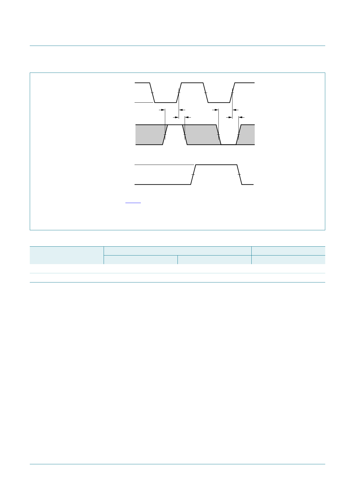
VI
CP input
GND
VI
Dn input
GND
VM
t su
th
VM
t su
th
VOH
Qn output
VOL
VM
mna767
Fig 9.
Measurement points are given in Table 8.
The shaded areas indicate when the input is permitted to change for predictable output performance.
VOL and VOH are typical voltage output levels that occur with the output load.
Data set-up and hold times data input (Dn)
Table 8. Measurement points
Type
Input
74HC273-Q100
74HCT273-Q100
VI
VCC
3V
VM
0.5VCC
1.3 V
Output
VM
0.5VCC
1.3 V
74HC_HCT273_Q100
Product data sheet
All information provided in this document is subject to legal disclaimers.
Rev. 1 — 19 June 2013
© NXP B.V. 2013. All rights reserved.
11 of 19
11 Page | ||
| Páginas | Total 19 Páginas | |
| PDF Descargar | [ Datasheet 74HCT273-Q100.PDF ] | |
Hoja de datos destacado
| Número de pieza | Descripción | Fabricantes |
| 74HCT273-Q100 | Octal D-type flip-flop | NXP Semiconductors |
| Número de pieza | Descripción | Fabricantes |
| SLA6805M | High Voltage 3 phase Motor Driver IC. |
Sanken |
| SDC1742 | 12- and 14-Bit Hybrid Synchro / Resolver-to-Digital Converters. |
Analog Devices |
|
DataSheet.es es una pagina web que funciona como un repositorio de manuales o hoja de datos de muchos de los productos más populares, |
| DataSheet.es | 2020 | Privacy Policy | Contacto | Buscar |
