|
|
|
PDF HS-303CEH Data sheet ( Hoja de datos )
| Número de pieza | HS-303CEH | |
| Descripción | Radiation Hardened BiCMOS Dual SPDT Analog Switch | |
| Fabricantes | Intersil | |
| Logotipo | ||
Hay una vista previa y un enlace de descarga de HS-303CEH (archivo pdf) en la parte inferior de esta página. Total 10 Páginas | ||
|
No Preview Available !
DATASHEET
Radiation Hardened BiCMOS Dual SPDT Analog Switch
HS-303CEH
The HS-303CEH is an analog switch and a monolithic device
that is fabricated using Intersil’s dielectrically isolated
Radiation Hardened Silicon Gate (RSG) process technology to
insure latch-up free operation. It is pinout compatible and
functionally equivalent to the HS-303RH. This switch offers
low-resistance switching performance for analog voltages up
to the supply rails. ON-resistance is low and stays reasonably
constant over the full range of operating voltage and current.
ON-resistance also stays reasonably constant when exposed to
radiation. Break-before-make switching is controlled by 5V
digital inputs. The HS-303CEH can operate with rails of ±15V.
Specifications
The Detailed Electrical Specifications for the HS-303CEH is
contained in SMD 5962-95813.
Features
• QML, per MIL-PRF-38535
• No latch-up, dielectrically isolated device islands
• Pinout and functionally compatible with Intersil HS-303RH
series analog switches
• Analog signal range equal to the supply voltage range
• Low leakage . . . . . . . . . . . . . . . . . . . . . 150nA (max, post-rad)
• Low rON . . . . . . . . . . . . . . . . . . . . . . . . . . . 60Ω (max, post-rad)
• Low standby supply current . . . . . . . ±150µA (max, post-rad)
• Radiation assurance
- High dose rate (50 to 300rad(Si)/s) . . . . . . . . 100krad(Si)
- Low dose rate (0.01rad(Si)/s) . . . . . . . . . . . . . 50krad(Si)*
• Single event effects
- For LET = 60MeV-mg/cm2 at 60° incident angle,
<150pC charge transferred to the output of an off switch
* Product capability established by initial characterization. The
EH version is acceptance tested on a wafer-by-wafer basis to
50krad(Si) at low dose rate.
S
IN N P
D
LOGIC
0
1
FIGURE 1. LOGIC CIRCUIT
TABLE 1. TRUTH TABLE
SW1 AND SW2
SW3 AND SW4
OFF ON
ON OFF
16
14
12
10
8
6
4
2
0
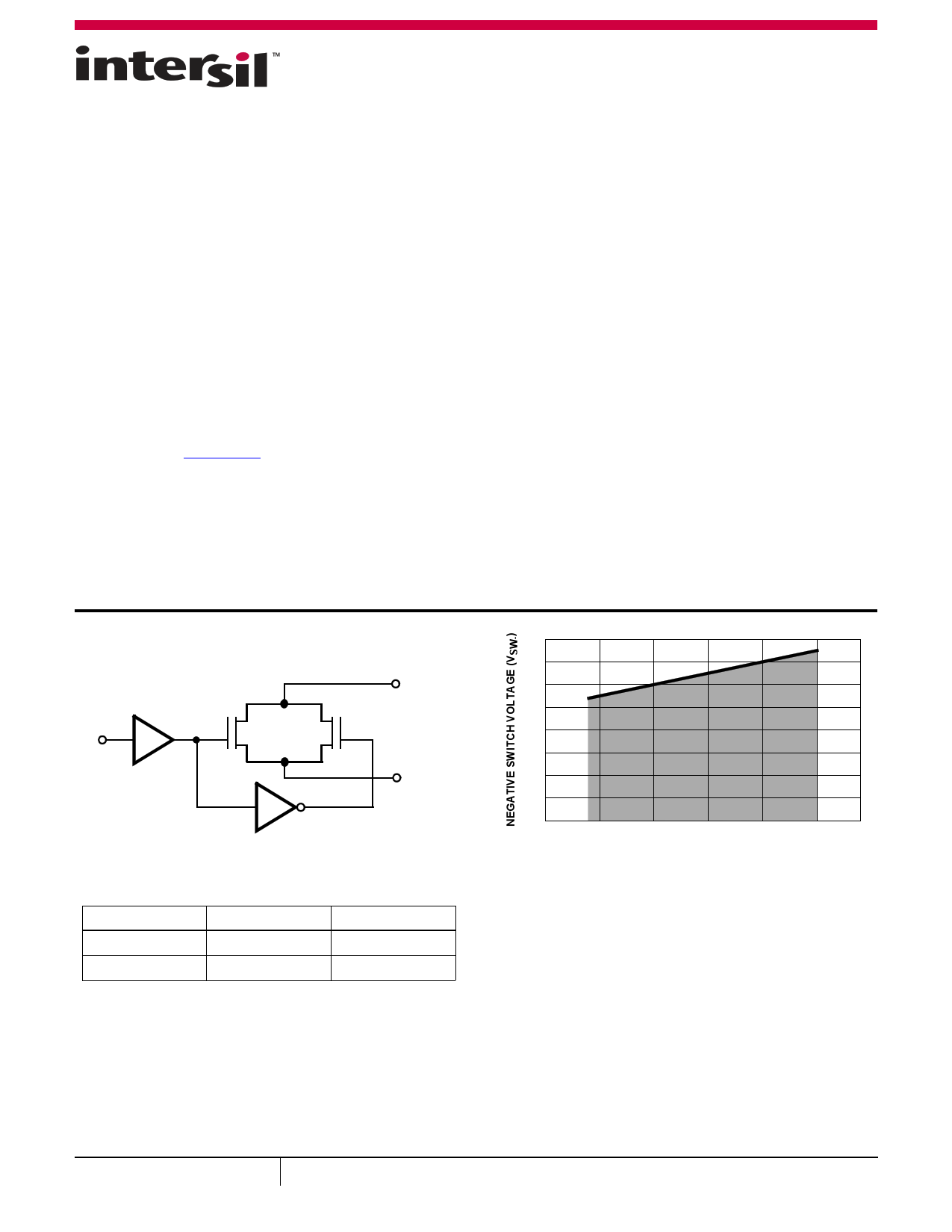
10 11 12 13 14 15
NEGATIVE SUPPLY VOLTAGE (V-)
FIGURE 2. RECOMMENDED OPERATING AREA IN GREY
March 4, 2015
FN8399.3
1
CAUTION: These devices are sensitive to electrostatic discharge; follow proper IC Handling Procedures.
1-888-INTERSIL or 1-888-468-3774 |Copyright Intersil Americas LLC 2012, 2013, 2015. All Rights Reserved
Intersil (and design) is a trademark owned by Intersil Corporation or one of its subsidiaries.
All other trademarks mentioned are the property of their respective owners.
1 page 
HS-303CEH
Post Radiation Characteristics VSUPPLY = ±15V unless otherwise specified. This data is typical test data post radiation exposure
at a rate of <10mrad(Si)/s. This data is intended to show typical parameter shifts due to total ionizing dose (low dose radiation). TA= +25°C.
SYMBOL
PARAMETER
TEST CONDITIONS
0k 25k 50k 75k 100k UNITS
+rDS(ON)
-rDS(ON)
+IS(OFF)
-IS(OFF)
+ID(OFF)
-ID(OFF)
+ID(ON)
“Switch On” Resistance
“Switch On” Resistance
Leakage Current into Source of an
“OFF” Switch
Leakage Current into Source of an
“OFF” Switch
Leakage Current into Drain of an “OFF”
Switch
Leakage Current into Drain of an “OFF”
Switch
Leakage Current from an “ON” Driver
into the Switch (Drain and Source)
VD = 10V, IS = -10mA
VD = -10V, IS = 10mA
VS = +14V, VD = -14V
VS = +15V, VD = -15V
VS = -14V, VD = +14V
VS = -15V, VD = +15V
VS = +14V, VD = -14V
VS = +15V, VD = -15V
VS = -14V, VD = +14V
VS = -15V, VD = +15V
VS = +14V, VD = +14V
33.57
27.56
-0.30
-0.006
0.32
0.004
-0.36
-0.001
0.34
0.0004
-0.25
34.39 34.37 34.75 34.65
28.37 28.48 28.92 28.77
-0.26 -0.36 -0.55 -0.47
-0.002 -0.002 -0.003 -0.002
0.45 0.75 1.05 0.94
0.003 0.003 0.003 0.002
-0.22 -0.25 -0.46 -0.40
-0.001 -0.001 -0.001 -0.002
0.43 0.69 1.02 0.92
0.0008 0.0011 0.0014 0.0018
-0.26 -0.36 -0.55 -0.65
Ω
Ω
nA
µA
nA
µA
nA
µA
nA
µA
nA
-ID(ON)
IAL
IAH
I+
I-
tOPEN
tON
tOFF
Leakage Current from an “ON” Driver
into the Switch (Drain and Source)
Low Level Input Address Current
High Level Input Address Current
Positive Supply Current
Negative Supply Current
Break-before-make Time Delay
Switch Turn “ON” Time
Switch Turn “OFF” Time
VS = -14V, VD = -14V
All Channels VA = 0.8V
All Channels VA = 4.0V
All Channels VA = 0.8V
VA1 = 0V, VA2 = 4V
VA1 = 4V, VA2 = 0V
All Channels VA = 0.8V
VA1 = 0V, VA2 = 4V
VA1 = 4V, VA2 = 0V
RL = 300Ω, VS = 3V, VAH = 5V, VAL = 0V
RL = 300Ω, VS = 3V, VAH = 4V, VAL = 0V
RL = 300Ω, VS = 3V, VAH = 4V, VAL = 0V
0.17
0.19
1.72
54
185
0.15
0.30
0.87
51
146
0.26
0.23
0.83
50
129
0.45
0.71
0.28
49
116
0.40
0.48
1.31
50
106
-0.011
-0.013
-0.015 -0.011 -0.019 -0.022
-0.016 -0.017 -0.019 -0.014
42.58
221.03
188.62
50.84 55.63 56.74 58.06
229.24 240.85 249.79 256.37
184.65 182.27 184.06 182.45
nA
nA
nA
µA
µA
µA
µA
ns
ns
ns
Submit Document Feedback
5
FN8399.3
March 4, 2015
5 Page | ||
| Páginas | Total 10 Páginas | |
| PDF Descargar | [ Datasheet HS-303CEH.PDF ] | |
Hoja de datos destacado
| Número de pieza | Descripción | Fabricantes |
| HS-303CEH | Radiation Hardened BiCMOS Dual SPDT Analog Switch | Intersil |
| Número de pieza | Descripción | Fabricantes |
| SLA6805M | High Voltage 3 phase Motor Driver IC. |
Sanken |
| SDC1742 | 12- and 14-Bit Hybrid Synchro / Resolver-to-Digital Converters. |
Analog Devices |
|
DataSheet.es es una pagina web que funciona como un repositorio de manuales o hoja de datos de muchos de los productos más populares, |
| DataSheet.es | 2020 | Privacy Policy | Contacto | Buscar |