|
|
|
PDF PALCE16V8H-15 Data sheet ( Hoja de datos )
| Número de pieza | PALCE16V8H-15 | |
| Descripción | EE CMOS Universal Programmable Array Logic | |
| Fabricantes | Advanced Micro Devices | |
| Logotipo | ||
Hay una vista previa y un enlace de descarga de PALCE16V8H-15 (archivo pdf) en la parte inferior de esta página. Total 30 Páginas | ||
|
No Preview Available !
-
PALCE16V8H-15/25
EE CMOS Universal Programmable Array Logic
Advanced
Micro
Devices
DISTINCTIVE CHARACTERISTICS
• Pin, function and fuse-map compatible with all
20-pln GAL® devices
• Electrically erasable CMOS technology
provides reconfigurable logic and full
testability
• High speed CMOS technology
- 15-ns propagation delay for "-15" version
- 25-ns propagation delay for "-25" version
• Direct plug-in replacement for the PAL16R8
series and most of the PAL1OH8 series
• Outputs programmable as registered or
combinatorial in any combination
GENERAL DESCRIPTION
The PALCE16V8 is an advanced PAL® device built with
low-power, high-speed, electrically-erasable CMOS
technology. It is functionally compatible with all 20-pin
GAL devices. The macrocells provide a universal device
architecture. ThePALCE16V8 will directly replace the
PAL16R8 and PAL1OH8 series devices, with the excep-
tion of the PAL16C1.
Device logic is automatically configured according to the
user's design specification. Design is simplified by
PALASM design software, allowing automatic creation
of a programming file based on Boolean or state equa-
tions. PALASM software also verifies the design and
can provide test vectors for the finished device. Pro-
gramming can be accomplished on standard PAL
device programmers.
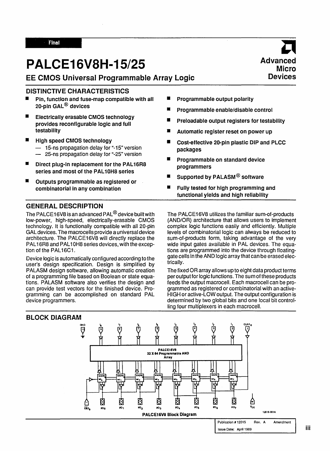
BLOCK DIAGRAM
• Programmable output polarity
• Programmable enable/disable control
• Preloadable output registers for testability
• Automatic register reset on power up
• Cost-effective 20-pin plastic DIP and PLCC
packages
• Programmable on standard device
programmers
• Supported by PALASM® software
• Fully tested for high programming and
functional yields and high reliability
The PALCE16V8 utilizes the familiar sum-of-products
(AND/OR) architecture that allows users to implement
complex logic functions easily and efficiently. Multiple
levels of combinatorial logic can always be reduced to
sum-of-products form, taking advantage of the very
wide input gates available in PAL devices. The equa-
tions are programmed into the device through floating-
gate cells in the AND logic array that can be erased elec-
trically.
The fixed OR array allows up to eight data product terms
per output for logic functions. The su m of these products
feeds the output macrocell. Each macrocell can be pro-
grammed as registered or combinatorial with an active-
HIGH or active-LOW output. The output configuration is
determined by two global bits and one local bit control-
ling four multiplexers in each macrocell.
PALCE16V8 Block Diagram
12015-0011<
Publication # 12015 Rev. A
Issue Date: April 1989
Amendment
iii
1 page 
Configuration Options
Each macrocell can be configured as one of the follow-
ing: registered output, combinatorial output or dedicated
input. In the registered output configuration, the output
buffer is enabled by theOE pin. In the combinatorial con-
figuration, the buffer is either controlled by a product
term or always enabled. In the dedicated input configu-
ration, it is always disabled. With the exception of MCo
and MC7, a macrocell configured as a dedicated input
derives the input signal from an adjacent 110. MCo
derives its input from pin 11 (DE) and MC7 from pin 1
(ClK).
The macrocell configurations are controlled by bits
stored in the configuration control word. It contains 2
global bits (SGO and SG1) and 16 local bits (SlOo
through Sl07 and Sl1 0 through Sl17). SGO determines
whether registers will be allowed. SG1 determines
whether the PAlCE16V8 will emulate a 16R8 family or a
PAL1OH8 family device. SlOx, in conjunction with SG1,
selects the configuration of the macrocell, and Sl1 xsets
the output as either active lOW or active HIGH for the
individual macrocell.
The configuration bits work by acting as control inputs
forthe multiplexers in the macrocell. There are four mul-
tiplexers: a product term input, an enable select, an out-
put select, and a feedback select multiplexer. SG1 and
SlOx are the control signals for all four multiplexers. In
addition, SlO forthe adjacent 110 is a control input to the
feedback multiplexer. In MCo and MC7, SGO replaces
SG1 on the feedback multiplexer. This accommodates
ClK being the adjacent pin for MC7 and DE for MCo•
Registered Output Configuration
The control bit settings are SGO =0, SG1 =1 and SlOx =
O. There is only one registered configuration. All eight
product terms are available as inputs to the OR gate.
Data polarity is determined by Sl1 x. The flip-flop is
loaded on the lOW to HIGH transition of ClK. The feed-
back path is from Q on the register. The output buffer is
enabled by OE.
Combinatorial Configurations
The PAlCE16V8 has three combinatorial output con-
figurations: dedicated output in a non-registered device,
110 in a non-registered device and 110 in a registered de-
vice.
Dedicated Output In a Non-Registered-
Device
The control bit settings are SGO =1, SG1 = 0 and SlOx =
O. All eight product terms are available to the OR gate.
Because the macrocell is a dedicated output, the feed-
back is not used. Because ClK andOE are not used in a
non-registered device, pins 1 and 11 are available as in-
put Signals. Pin 1 will use the feedback path of MC7 and
pin 11 will use the feedback path of MCo.
Combinatorial I/O In a Non-Registered
Device
The control settings are SGO = 1, SG1 =1, and SlOx =1.
Only seven product terms are available to the OR gate.
The eighth product term is used to enable the output
buffer. The signal at the 110 pin is fed back to the AND
array via the feedback multiplexer. This allows the pin to
be used as an input.
.
Because ClK and DE are not used in a non-registered
device, pins 1 and 11 are available as inputs. Pin 1 will
use the feedback path of MC7 and pin 11 will use the
feedback path of MCo•
Combinatorial I/O in a Registered Device
The control bit settings are SGO =0, SG1 =1 and SlOx =
1. Only seven product terms are available to the OR
gate. The eighth product term is used as the output
enable. The feedback signal is the corresponding 110
Signal.
Dedicated Input Configuration
The control bit settings are SGO = 1, SG1 = 0 and SlOx =
1. The output buffer is disabled. Except for MCoand MC7
the feedback signal is an adjacent 110. For MCo and MC7
the feedback signals are pins 1 and 11. These configu-
rations are summarized in Table 1 and illustrated in Fig-
ure 2.
.
Macrocell Configuration
SGO SG1 SLOx Cell Configuration Devices Emulated
Device Uses Registers
0 1 0 Registered Output PAL 16RB, 16R6,
16R4
0 1 1 Combinatorial 1/0 PAl16R6,16R4
Device Uses No Registers
1 0 0 Combinatorial
PAL1OHB, 12H6,
Output
14H4, 16H2, 10lB,
12l6, 14l4, 16L2
1 0 1 Input
PAL12H6,14H4,
16H2, 12l6, 14L4,
1612
1 1 1 Combinatorial 1/0 PAL16LB
Programmable Output Polarity
The polarity of each macrocell can be active HIGH or
active lOW, either to match output signal needs or to
reduce product terms. Programmable polarity allows
Boolean expressions to be written in their most compact
form (true or inverted), and the output can still be of the
desired polarity. It can also save "DeMorganizing"
efforts.
Selection is through a programmable bit Sl1 x which
controls an exclusive-OR Gate at the output of the ANDI
OR logic. The output is active-HIGH if SL1x is "1" and
active-lOW if Sl1 x is "0".
PALCE16V8H-15/25
vii
5 Page 
SWITCHING CHARACTERISTICS over Commercial operating range (Note 1)
Parameter Parameter
Symbol
Description
-15
Min. Max.
-25
Min. Max.
tpo Input or Feedback to Combinatorial Output (Note 2)
15
25
ts Setup Time from Input or Feedback to Clock 12
15
tH Hold Time
00
tco Clock to Output
10 12
tCF Clock to Feedback
8 10
tWl
Width of Clock
LOW
8 10
tWH
HIGH
8 10
Maximum
fMAx Frequency
(Note 3)
External Feedback 1/(ts+tco)
Internal Feedback 1/(tS+tCF)
No Feedback 1/(tWH+tWL)
45.5
50.0
62.5
37
40
40
tpzx OE to Output Enable (Note 4)
15 20
tpxz OE to Output Disable (Note 4)
15 20
tEA Input to Output Enable (Notes 4 and 5)
15 25
tER Input to Output Disable (Notes 4 and 5)
15 25
Unit
ns
ns
ns
ns
ns
ns
MHz
ns
ns
ns
ns
Notes:
1. Commercial Test Conditions: Rl = 200n, R2 = 390n (see switching test circuit).
2. tPD is tested with 8 1 closed and CL= 50pF (including jig capacitance). V1H = 3V, V1L = OV, VOH = VOL = 1.5V.
3. These parameters are not 100% tested, but are calculated at initial characterization and at any time the design is modified
where frequency may be affected.
4. For three-state outputs, enable times are tested with CL= 50pF to the 1.5V level; 8 1 is open for high-impedance to HIGH
tests and closed for high-impedance to LOW tests. Output disable times are tested with CL= 5pF. HIGH to high-
impedance tests are made to an output voltage of VOH -O.5V with 8 1 open; LOW to high-impedance tests are made to an
output voltage of VOL to +0.5V with 8 1 closed.
5. Equivalent function to tpzx, tpxz but using product term control.
PALCE16V8H-15/25
xiii
11 Page | ||
| Páginas | Total 30 Páginas | |
| PDF Descargar | [ Datasheet PALCE16V8H-15.PDF ] | |
Hoja de datos destacado
| Número de pieza | Descripción | Fabricantes |
| PALCE16V8H-15 | EE CMOS Universal Programmable Array Logic | Advanced Micro Devices |
| Número de pieza | Descripción | Fabricantes |
| SLA6805M | High Voltage 3 phase Motor Driver IC. |
Sanken |
| SDC1742 | 12- and 14-Bit Hybrid Synchro / Resolver-to-Digital Converters. |
Analog Devices |
|
DataSheet.es es una pagina web que funciona como un repositorio de manuales o hoja de datos de muchos de los productos más populares, |
| DataSheet.es | 2020 | Privacy Policy | Contacto | Buscar |