|
|
|
PDF CY7C1362V25 Data sheet ( Hoja de datos )
| Número de pieza | CY7C1362V25 | |
| Descripción | 256K x 36/256K x 32/512K x 18 Pipelined SRAM | |
| Fabricantes | Cypress Semiconductor | |
| Logotipo | ||
Hay una vista previa y un enlace de descarga de CY7C1362V25 (archivo pdf) en la parte inferior de esta página. Total 30 Páginas | ||
|
No Preview Available !
PRELIMINARY
CY7C1360V25
CY7C1362V25
CY7C1364V25
256K x 36/256K x 32/512K x 18 Pipelined SRAM
Features
• Supports 200-MHz bus
• Fully registered inputs and outputs for pipelined
operation
• Single 2.5V power supply
• Fast clock-to-output times
— 3.1 ns (for 200-MHz device)
— 3.5 ns (for 166-MHz device)
— 4.0 ns (for 133-MHz device
— 5.0 ns (for 100-MHz device
• User-selectable burst counter supporting Intel®
Pentium® interleaved or linear burst sequences
• Separate processor and controller address strobes
• Synchronous self-timed writes
• Asynchronous output enable
• Available as a 100-pin TQFP or 119 BGA
• “ZZ” Sleep Mode option and Stop Clock option
Functional Description
The CY7C1360V25, CY7C1364V25 and CY7C1362V25 are
2.5V, 256K x 36, 256K x 32 and 512K x 18 synchronous-pipe-
lined cache SRAM, respectively. They are designed to support
zero wait state secondary cache with minimal glue logic.
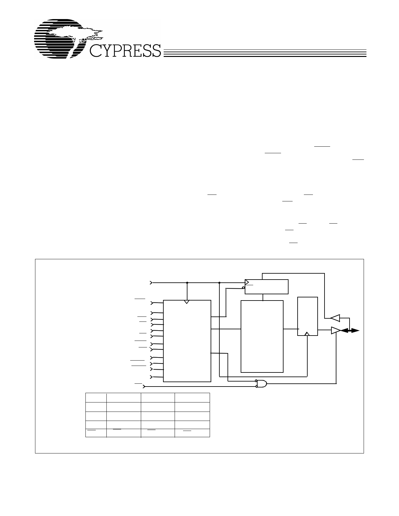
Logic Block Diagram
All synchronous inputs pass through input registers controlled
by the rising edge of the clock. All data outputs pass through
output registers controlled by the rising edge of the clock. Max-
imum access delay from the clock rise is 3.1 ns (200-MHz
device).
The CY7C1360V25/CY7C1364V25/CY7C1362V25 supports
either the interleaved burst sequence used by the Intel Pen-
tium processor or a linear burst sequence used by processors
such as the PowerPC™. The burst sequence is selected
through the MODE pin. Accesses can be initiated by assert-
ing either the Processor Address Strobe (ADSP) or the Con-
troller Address Strobe (ADSC) at clock rise. Address advance-
ment through the burst sequence is controlled by the ADV
input. A 2-bit on-chip wraparound burst counter captures the
first address in a burst sequence and automatically increments
the address for the rest of the burst access.
Byte write operations are qualified with the Byte Write Select
(BWa,b,c,d for 1360V25/1364V25 and BWa,b for 1362V25) in-
puts. A Global Write Enable (GW) overrides all byte write in-
puts and writes data to all four bytes. All writes are conducted
with on-chip synchronous self-timed write circuitry.
Three synchronous Chip Selects (CE1, CE2, CE3) and an
asynchronous Output Enable (OE) provide for easy bank se-
lection and output three-state control. In order to provide prop-
er data during depth expansion, OE is masked during the first
clock of a read cycle when emerging from a deselected state.
CLK
AX
DQX
DPX
BWX
ADV
Ax
GW
CCEE12
CE3
BWE
BWx
MODE
ADSP
ADSC
ZZ
OE
CONTROL
and WRITE
LOGIC
1360V25
A[17:0]
DQa,b,c,d
DPa,b,c,d
BWa,b,c,d
1362V25
A[18:0]
DQa,b
DPa,b
BWa,b
1364V25
A[18:0]
DQa,b
NC
BWa,b
CE
DaDta-In
Q
REG.
256Kx36/
512Kx18
MEMORY
ARRAY
DQx
DPx
Intel and Pentium are registered trademarks of Intel Corporation.
PowerPC is a trademark of IBM Corporation.
Cypress Semiconductor Corporation • 3901 North First Street • San Jose • CA 95134 • 408-943-2600
December 3, 1999
1 page 
PRELIMINARY
CY7C1360V25
CY7C1362V25
CY7C1364V25
Pin Definitions (100-Pin TQFP) (continued)
x18 Pin Locations x36 Pin Locations Name
85 85
ADSC
31 31
MODE
64 64
ZZ
(a) 58, 59, 62, 63,
68, 69, 72, 73
(b) 8, 9, 12, 13, 18,
19, 22, 23
(a) 52, 53, 56–59,
62, 63
(b) 68, 69, 72–75,
78, 79
(c) 2, 3, 6–9, 12, 13
(d) 18, 19, 22–25,
28, 29
DQa
DQb
DQc
DQd
74, 24
51, 80, 1, 30
NC,DQPa
NC,DQPb
NC,DQPc
NC,DQPd
15, 41, 65, 91
15, 41, 65, 91
VDD
17, 40, 67, 90
17, 40, 67, 90
VSS
4, 11, 20, 27, 54,
61, 70, 77
5, 10, 21, 26, 55,
60, 71, 76
1, 2, 3, 6, 7, 14, 16,
25, 28, 29, 30, 51,
52, 53, 56, 57, 66,
75, 78, 79, 95, 96
42
4, 11, 20, 27, 54, 61,
70, 77
5, 10, 21, 26, 55, 60,
71, 76
16, 66
42
VDDQ
VSSQ
NC
DNU
38, 39
38, 39
DNU
I/O
Input-
Synchronous
Input-
Static
Input-
Asynchronous
I/O-
Synchronous
I/O-
Synchronous
Power Supply
Ground
I/O Power
Supply
I/O Ground
-
Description
Address Strobe from Controller, sampled on the ris-
ing edge of CLK. When asserted LOW, A[x:0] is cap-
tured in the address registers. A[1:0] are also loaded
into the burst counter. When ADSP and ADSC are
both asserted, only ADSP is recognized.
Selects Burst Order. When tied to GND selects lin-
ear burst sequence. When tied to VDDQ or left float-
ing selects interleaved burst sequence. This is a
strap pin and should remain static during device
operation.
ZZ “sleep” Input. This active HIGH input places the
device in a non-time critical “sleep” condition with
data integrity preserved.
Bidirectional Data I/O lines. As inputs, they feed
into an on-chip data register that is triggered by the
rising edge of CLK. As outputs, they deliver the data
contained in the memory location specified by A
during the previous clock rise of the read cycle. The
direction of the pins is controlled by OE. When OE
is asserted LOW, the pins behave as outputs.
When HIGH, DQa and DPa are placed in a
three-state condition.
Bidirectional Data I/O lines. As inputs, they feed
into an on-chip data register that is triggered by the
rising edge of CLK. As outputs, they deliver the data
contained in the memory location specified by A
during the previous clock rise of the read cycle. The
direction of the pins is controlled by OE. When OE
is asserted LOW, the pins behave as outputs.
When HIGH, DQx and DPx are placed in a
three-state condition.
These are not connect pins on the CY7C1364.
Power supply inputs to the core of the device.
Should be connected to 2.5V power supply.
Ground for the core of the device. Should be con-
nected to ground of the system.
Power supply for the I/O circuitry. Should be con-
nected to a 2.5V power supply.
Ground for the I/O circuitry. Should be connected
to ground of the system.
No Connects.
Do Not Use Pin. This pin is used for the expansion
to the 16M density.
Do Not Use Pins. These pins should be left floating
or tied to VSS.
5
5 Page 
Write Cycle Description[1, 2, 3]
Function (1360/1364)
Read
Read
Write Byte 0-DQa
Write Byte 1-DQb
Write Bytes 1, 0
Write Byte 2 - DQc
Write Bytes 2, 0
Write Bytes 2, 1
Write Bytes 2, 1, 0
Write Byte 3 - DQd
Write Bytes 3, 0
Write Bytes 3, 1
Write Bytes 3, 1, 0
Write Bytes 3, 2
Write Bytes 3, 2, 0
Write Bytes 3, 2, 1
Write All Bytes
Write All Bytes
Function (1362)
Read
Read
Write Byte 0 - DQ[7:0] and DP0
Write Byte 1 - DQ[15:8] and DP1
Write All Bytes
Write All Bytes
PRELIMINARY
CY7C1360V25
CY7C1362V25
CY7C1364V25
GW
BWE
BWd
11X
101
101
101
101
101
101
101
101
100
100
100
100
100
100
100
100
0XX
GW BWE
11
10
10
10
10
0X
BWc
X
1
1
1
1
0
0
0
0
1
1
1
1
0
0
0
0
X
BWb
X
1
1
0
0
1
1
0
0
1
1
0
0
1
1
0
0
X
BWa
X
1
0
1
0
1
0
1
0
1
0
1
0
1
0
1
0
X
BWb
X
1
1
0
0
X
BWa
X
1
0
1
0
X
11
11 Page | ||
| Páginas | Total 30 Páginas | |
| PDF Descargar | [ Datasheet CY7C1362V25.PDF ] | |
Hoja de datos destacado
| Número de pieza | Descripción | Fabricantes |
| CY7C1362V25 | 256K x 36/256K x 32/512K x 18 Pipelined SRAM | Cypress Semiconductor |
| Número de pieza | Descripción | Fabricantes |
| SLA6805M | High Voltage 3 phase Motor Driver IC. |
Sanken |
| SDC1742 | 12- and 14-Bit Hybrid Synchro / Resolver-to-Digital Converters. |
Analog Devices |
|
DataSheet.es es una pagina web que funciona como un repositorio de manuales o hoja de datos de muchos de los productos más populares, |
| DataSheet.es | 2020 | Privacy Policy | Contacto | Buscar |