|
|
PDF CY7C4121KV13 Data sheet ( Hoja de datos )
| Número de pieza | CY7C4121KV13 | |
| Descripción | 144-Mbit QDR-IV HP SRAM | |
| Fabricantes | Cypress Semiconductor | |
| Logotipo | ||
Hay una vista previa y un enlace de descarga de CY7C4121KV13 (archivo pdf) en la parte inferior de esta página. Total 30 Páginas | ||
|
No Preview Available !
CY7C4121KV13/CY7C4141KV13
144-Mbit QDR™-IV HP SRAM
144-Mbit QDR™-IV HP SRAM
Features
■ 144-Mbit density (8M ×18, 4M ×36)
■ Total Random Transaction Rate [1] of 1334 MT/s
■ Maximum operating frequency of 667 MHz
■ Read latency of 5.0 clock cycles and write latency of 3.0 clock
cycles
■ Two-word burst on all accesses
■ Dual independent bidirectional data ports
❐ Double data rate (DDR) data ports
❐ Supports concurrent read/write transactions on both ports
■ Single address port used to control both data ports
❐ DDR address signaling
■ Single data rate (SDR) control signaling
■ High-speed transceiver logic (HSTL) and stub series
terminated logic (SSTL) compatible signaling (JESD8-16A
compliant)
❐ I/O VDDQ = 1.2 V ± 50 mV or 1.25 V ± 50 mV
■ Pseudo open drain (POD) signaling (JESD8-24 compliant)
❐ I/O VDDQ = 1.1 V ± 50 mV or 1.2 V ± 50 mV
■ Core voltage
❐ VDD = 1.3 V ±40 mV
■ On-die termination (ODT)
❐ Programmable for clock, address/command, and data inputs
■ Internal self-calibration of output impedance through ZQ pin
■ Bus inversion to reduce switching noise and power
❐ Programmable on/off for address and data
■ Address bus parity error protection
■ Training sequence for per-bit deskew
■ On-chip error correction code (ECC) to reduce soft error rate
(SER)
■ JTAG 1149.1 test access port (JESD8-26 compliant)
❐ 1.3-V LVCMOS signaling
■ Available in 361-ball FCBGA Pb-free package (21 × 21 mm)
Selection Guide
Description
Maximum operating frequency
Maximum operating current
Configurations
CY7C4121KV13 – 8M ×18
CY7C4141KV13 – 4M ×36
Functional Description
The QDR™-IV HP (High-Performance) SRAM is a
high-performance memory device that has been optimized to
maximize the number of random transactions per second by the
use of two independent bidirectional data ports.
These ports are equipped with DDR interfaces and designated
as port A and port B respectively. Accesses to these two data
ports are concurrent and completely independent of each other.
Access to each port is through a common address bus running
at DDR. The control signals are running at SDR and determine
if a read or write should be performed.
There are three types of differential clocks:
■ (CK, CK#) for address and command clocking
■ (DKA, DKA#, DKB, DKB#) for data input clocking
■ (QKA, QKA#, QKB, QKB#) for data output clocking
Addresses for port A are latched on the rising edge of the input
clock (CK), and addresses for port B are latched on the falling
edge of the input clock (CK).
The QDR-IV HP SRAM device is offered in a two-word burst
option and is available in ×18 and ×36 bus width configurations.
For a ×18 bus width configuration, there are 22 address bits, and
for a ×36 bus width configuration, there are 21 address bits
respectively.
An on-chip ECC circuitry detects and corrects all single-bit
memory errors, including those induced by soft-error events,
such as cosmic rays and alpha particles. The resulting SER of
these devices is expected to be less than 0.01 FITs/Mb, a
four-order-of-magnitude improvement over previous generation
SRAMs.
For a complete list of related resources, click here.
QDR-IV
1334 (MT/s)
667
×18 2500
×36 3200
QDR-IV
1266 (MT/s)
633
2400
2950
QDR-IV
1200 (MT/s)
600
2300
2700
Unit
MHz
mA
Note
1. Random Transaction Rate (RTR) is defined as the number of fully random memory accesses (reads or writes) that can be performed on the memory. RTR is measured
in million transactions per second.
Cypress Semiconductor Corporation • 198 Champion Court
Document Number: 001-79343 Rev. *P
• San Jose, CA 95134-1709 • 408-943-2600
Revised July 29, 2016
1 page 
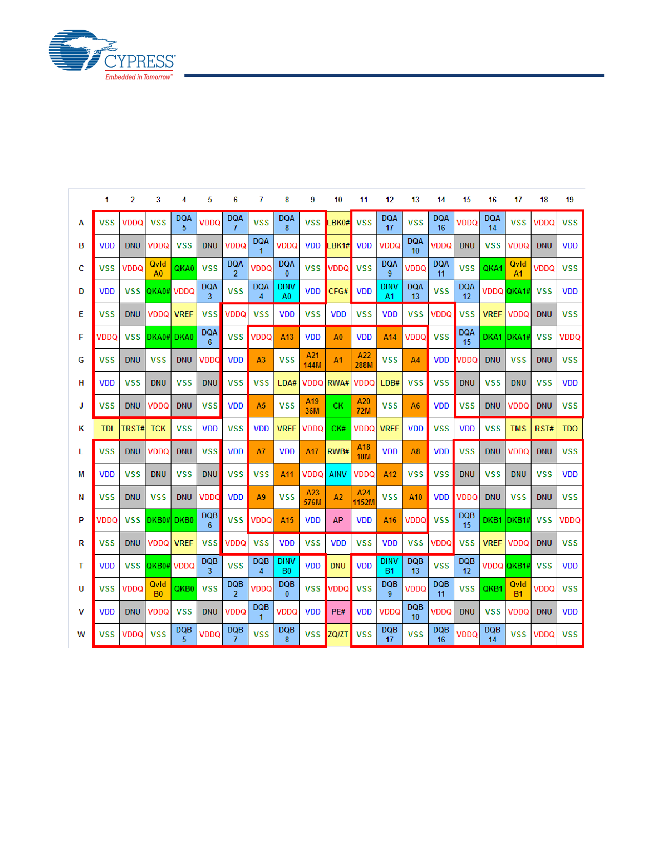
Pin Configurations
CY7C4121KV13/CY7C4141KV13
Figure 1. 361-ball FCBGA Pinout
CY7C4121KV13 (8M ×18)
Document Number: 001-79343 Rev. *P
Page 5 of 45
5 Page 
CY7C4121KV13/CY7C4141KV13
Typically, after a reset sequence, the system starts to perform a
training sequence, involving the steps outlined in the following
section.
However, RST# may be asserted at any time by the system and
the system may wish to initiate normal read/write operations after
a reset sequence, without going through another training
sequence. The chip should be able to accept normal read/write
operations immediately following tRSH after the deassertion of
RST#.
PLL Reset Operation
The configuration registers contain a bit to reset the PLL.
Operating the QDR-IV HP SRAM device without the PLL
enabled is not supported—timing characteristics are not
guaranteed when the PLL is disabled. However, this bit is
intended to allow the system to reset the PLL locking circuitry.
Resetting the PLL is accomplished by first programming the PLL
Reset bit to 1 to disable the PLL, and then programming the bit
to 0 to enable the PLL. After these steps, the PLL will relock to
the input clock. A wait time of tPLL is required.
Operation Modes
The QDR-IV HP SRAM has three unique modes of operation:
1. Configuration
2. Loopback
3. Memory Access
These modes are defined by the level of the control signals
CFG#, LBK0#, LBK1#, LDA#, LDB#.
It is intended that these operations are mutually exclusive. In
other words, one operation mode cannot be performed
simultaneously with another operation mode.
There is no priority given for inadvertently asserting the control
signals at the wrong time. The internal chip behavior is not
defined for improper control signal assertion. The system must
strictly adhere to proper mode transitions, as defined in the
following sections, for proper device operation.
Configuration
A configuration operation mode is entered when the CFG# signal
is asserted. Memory Access or Loopback operations should not
be performed for a minimum of 32 clocks prior to entering this
mode.
While in this mode, the control signals LDB#, LBK0#, and LBK1#
must not be asserted. However, LDA# is used to perform the
actual Register Read and Write operations.
Memory Access or Loopback operations should not be
performed for a minimum of 32 clocks after exiting this mode.
Loopback
A loopback operation mode is entered when the LBK0# and/or
LBK1# signals are asserted. Memory Access or Configuration
operations should not be performed for a minimum of 32 clocks
prior to entering this mode.
Just after entering this mode, an additional 32 clocks are
required before the part is ready to accept toggling valid inputs
for training.
While in this mode, LDA# and LDB# may be toggled for training.
Memory Access or Configuration operations should not be
performed for a minimum of 32 clocks after exiting this mode.
Data inversion is not used during the Loopback mode. Even if
the configuration register has this feature enabled, it is
temporarily ignored during the Loopback mode.
Memory Access
If the control signals CFG#, LBK0#, and LBK1# are not asserted,
then the device is in the Memory Access mode. This mode is the
normal operating mode of the device.
While in this mode, a memory access cycle is performed when
the LDA# and/or LDB# signals are asserted. The control signals
CFG#, LBK0#, and LBK1# must not be asserted when
performing a memory access cycle.
A memory access should not be performed for a minimum of 32
clocks prior to leaving this mode.
Deskew Training Sequence
The QDR-IV HP SRAM provides support that allows a memory
controller to deskew signals for high-speed operation. The
memory controller provides the deskew function, if deskew is
desired. During the deskew operation, the QDR-IV HP SRAM
operates in a loopback mode.
Refer to the loopback timing diagram (Figure 15 on page 39).
Deskew is achieved in three steps:
1. Control/address deskew
2. Read data deskew
3. Write data deskew
Control/Address Deskew
Assert LBK0# to 0 and/or LBK1# to 0
The following 39 signals are looped back:
■ DKA0, DKA0#, DKA1, DKA1#
■ DKB0, DKB0#, DKB1, DKB1#
■ LDA#, RWA#, LDB#, RWB#
■ A[24:0], AINV, AP
The clock inputs DKA0, DKA0#, DKA1#, DKB0, DKB0#, DKB1,
and DKB1# are free-running clock inputs and should be
continuously running during the training sequence. In addition, a
wait time of tPLL is needed.
Refer to Table 1 on page 14 for the loopback signal mapping.
For each pin that is looped back, the input pin is sampled on both
the rising and falling edges using the input clock (CK/CK#).
The value output on the rising edge of the output clock
(QKA/QKA#) will be the value that was sampled on the rising
edge of the input clock.
The value output on the falling edge of the output clock
(QKA/QKA#) will be the inverted value that was sampled on the
falling edge of the input clock.
The delay from the input pins to the DQA outputs is tLBL, which
is 16 clocks.
Document Number: 001-79343 Rev. *P
Page 11 of 45
11 Page | ||
| Páginas | Total 30 Páginas | |
| PDF Descargar | [ Datasheet CY7C4121KV13.PDF ] | |
Hoja de datos destacado
| Número de pieza | Descripción | Fabricantes |
| CY7C4121KV13 | 144-Mbit QDR-IV HP SRAM | Cypress Semiconductor |
| Número de pieza | Descripción | Fabricantes |
| SLA6805M | High Voltage 3 phase Motor Driver IC. |
Sanken |
| SDC1742 | 12- and 14-Bit Hybrid Synchro / Resolver-to-Digital Converters. |
Analog Devices |
|
DataSheet.es es una pagina web que funciona como un repositorio de manuales o hoja de datos de muchos de los productos más populares, |
| DataSheet.es | 2020 | Privacy Policy | Contacto | Buscar |
