|
|
|
PDF CY7C09279V Data sheet ( Hoja de datos )
| Número de pieza | CY7C09279V | |
| Descripción | 3.3 V 16K / 32K / 64K x 16 / 18 Synchronous Dual-Port Static RAM | |
| Fabricantes | Cypress Semiconductor | |
| Logotipo | ||
Hay una vista previa y un enlace de descarga de CY7C09279V (archivo pdf) en la parte inferior de esta página. Total 25 Páginas | ||
|
No Preview Available !
CY7C09269V/79V/89V
CY7C09369V/89V
3.3 V 16K / 32K / 64K × 16 / 18
Synchronous Dual-Port Static RAM
3.3 V 16K / 32K / 64K × 16 / 18 Synchronous Dual-Port Static RAM
Features
■ True dual-ported memory cells that allow simultaneous access
of the same memory location
■ Six flow through/pipelined devices:
❐ 16K × 16 / 18 organization (CY7C09269V/369V)
❐ 32K × 16 organization (CY7C09279V)
❐ 64K × 16 / 18 organization (CY7C09289V/389V)
■ Three modes:
❐ Flow through
❐ Pipelined
❐ Burst
■ Pipelined output mode on both ports allows fast 100 MHz
operation
■ 0.35 micron CMOS for optimum speed and power
■ High speed clock to data access: 7.5[1], 9, 12 ns (max)
■ 3.3 V low operating power:
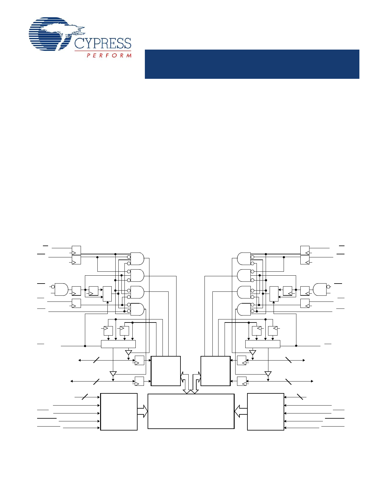
Logic Block Diagram
R/WL
UBL
❐ Active = 115 mA (typical)
❐ Standby = 10 A (typical)
■ Fully synchronous interface for easier operation
■ Burst counters increment addresses internally:
❐ Shorten cycle times
❐ Minimize bus noise
❐ Supported in flow through and pipelined modes
■ Dual chip enables easy depth expansion
■ Upper and lower byte controls for bus matching
■ Automatic power down
■ Commercial and industrial temperature ranges
■ Pb-free 100-pin TQFP package available
Functional Description
For a complete list of related documentation, click here.
R/WR
UBR
CE0L
CE1L
LBL
OEL
1
0
0/1
1 CE0R
0 CE1R
0/1 LBR
OER
FT/PipeL
[2]
I/O8/9L–I/O15/17L
1b 0b 1a 0a
0/1 b
a
8/9
[3]
I/O0L–I/O7/8L
8/9
[4] 14/15/16
A0L–A13/14/15L
CLKL
ADSL
Counter/
Address
Register
CNTENL
Decode
CNTRSTL
Notes
1. See Figure 4 on page 8 for Load Conditions.
2. I/O8–I/O15 for × 16 devices; I/O9–I/O17 for × 18 devices.
3. I/O0–I/O7 for × 16 devices. I/O0–I/O8 for × 18 devices.
4. A0–A13 for 16K; A0–A14 for 32K; A0–A15 for 64K devices.
I/O
Control
I/O
Control
True Dual-Ported
RAM Array
0a 1a 0b 1b
a b 0/1
8/9
FT/PipeR
[2]
I/O8/9R–I/O15/17R
Counter/
Address
Register
Decode
8/9 [3]
I/O0R–I/O7/8R
14/15/16
[4]
A0R–A13/14/15R
CLKR
ADSR
CNTENR
CNTRSTR
Cypress Semiconductor Corporation • 198 Champion Court
Document Number: 38-06056 Rev. *M
• San Jose, CA 95134-1709 • 408-943-2600
Revised March 21, 2016
1 page 
CY7C09269V/79V/89V
CY7C09369V/89V
Selection Guide
Specifications
fMAX2 (MHz) (Pipelined)
Max. Access Time (ns) (Clock to Data, Pipelined)
Typical Operating Current ICC (mA)
Typical Standby Current for ISB1 (mA) (Both Ports TTL
Level)
Typical Standby Current for ISB3 (A) (Both Ports CMOS
Level)
CY7C09269V/79V/89V
CY7C09369V/89V
-7[10]
83
7.5
155
25
10
CY7C09269V/79V/89V
CY7C09369V/89V
-9
67
9
135
20
10
CY7C09269V/79V/89V
CY7C09369V/89V
-12
50
12
115
20
10
Pin Definitions
Left Port
A0L–A15L
ADSL
CE0L, CE1L
CLKL
CNTENL
CNTRSTL
I/O0L–I/O17L
LBL
UBL
OEL
R/WL
FT/PIPEL
GND
NC
VCC
Right Port
Description
A0R–A15R
ADSR
Address Inputs (A0–A14 for 32K, A0–A13 for 16K devices).
Address Strobe Input. Used as an address qualifier. This signal must be asserted LOW to access
the part using an externally supplied address. Asserting this signal LOW also loads the burst counter
with the address present on the address pins.
CE0R,CE1R
CLKR
CNTENR
Chip Enable Input. To select either the left or right port, both CE0 AND CE1 must be asserted to their
active states (CE0 VIL and CE1 VIH).
Clock Signal. This input can be free running or strobed. Maximum clock input rate is fMAX.
Counter Enable Input. Asserting this signal LOW increments the burst address counter of its
respective port on each rising edge of CLK. CNTEN is disabled if ADS or CNTRST are asserted LOW.
CNTRSTR
Counter Reset Input. Asserting this signal LOW resets the burst address counter of its respective
port to zero. CNTRST is not disabled by asserting ADS or CNTEN.
I/O0R–I/O17R
LBR
Data Bus Input/Output (I/O0–I/O15 for × 16 devices).
Lower Byte Select Input. Asserting this signal LOW enables read and write operations to the lower
byte. (I/O0–I/O8 for × 18, I/O0–I/O7 for × 16) of the memory array. For read operations both the LB and
OE signals must be asserted to drive output data on the lower byte of the data pins.
UBR
OER
Upper Byte Select Input. Same function as LB, but to the upper byte (I/O8/9L–I/O15/17L).
Output Enable Input. This signal must be asserted LOW to enable the I/O data pins during read
operations.
R/WR
Read/Write Enable Input. This signal is asserted LOW to write to the dual port memory array. For
read operations, assert this pin HIGH.
FT/PIPER
Flow Through/Pipelined Select Input. For flow through mode operation, assert this pin LOW. For
pipelined mode operation, assert this pin HIGH.
Ground Input.
No Connect.
Power Input.
Note
10. See Figure 4 on page 8 for Load Conditions.
Document Number: 38-06056 Rev. *M
Page 5 of 25
5 Page 
CY7C09269V/79V/89V
CY7C09369V/89V
Switching Waveforms (continued)
Figure 7. Bank Select Pipelined Read [25, 26]
tCYC2
tCH2
tCL2
CLKL
tSA tHA
ADDRESS(B1)
A0
A1
A2
A3
tSC tHC
CE0(B1)
tCD2
tSC tHC tCD2
tCKHZ
A4
tCD2
DATAOUT(B1)
ADDRESS(B2)
tSA
CE0(B2)
DATAOUT(B2)
tSC
tHA
A0
A1
D0
tDC
A2
tSC
tHC
D1
tDC
A3
tCKLZ
A4
tHC
tCD2
tCKHZ
D2
tCKLZ
Figure 8. Left Port Write to Flow Through Right Port Read [27, 28, 29, 30]
A5
tCKHZ
D3
A5
tCD2
tCKLZ
D4
CLKL
R/WL
ADDRESSL
tSW tHW
tSA tHA
MATCH
tSD tHD
NO
MATCH
DATAINL
CLKR
VALID
tCCS
tCD1
R/WR
tSW tHW
tSA tHA
ADDRESSR
DATAOUTR
MATCH
tCWDD
tDC
NO
MATCH
VALID
tDC
tCD1
VALID
Notes
25. In this depth expansion example, B1 represents Bank #1 and B2 is Bank #2; Each Bank consists of one Cypress dual-port device from this datasheet.
ADDRESS(B1) = ADDRESS(B2).
26. UB, LB, OE and ADS = VIL; CE1(B1), CE1(B2), R/W, CNTEN, and CNTRST = VIH.
27. The same waveforms apply for a right port write to flow through left port read.
28. CE0, UB, LB, and ADS = VIL; CE1, CNTEN, and CNTRST = VIH.
29. OE = VIL for the Right Port, which is being read from. OE = VIH for the Left Port, which is being written to.
30. It tCCS maximum specified, then data from right port READ is not valid until the maximum specified for tCWDD. If tCCS>maximum specified, then data is not valid until
tCCS + tCD1. tCWDD does not apply in this case.
Document Number: 38-06056 Rev. *M
Page 11 of 25
11 Page | ||
| Páginas | Total 25 Páginas | |
| PDF Descargar | [ Datasheet CY7C09279V.PDF ] | |
Hoja de datos destacado
| Número de pieza | Descripción | Fabricantes |
| CY7C09279 | (CY7C09279 - CY7C09289) 32K/64K X 16/18 Synchronous Dual Port Static RAM | Cypress Semiconductor |
| CY7C09279V | 3.3 V 16K / 32K / 64K x 16 / 18 Synchronous Dual-Port Static RAM | Cypress Semiconductor |
| Número de pieza | Descripción | Fabricantes |
| SLA6805M | High Voltage 3 phase Motor Driver IC. |
Sanken |
| SDC1742 | 12- and 14-Bit Hybrid Synchro / Resolver-to-Digital Converters. |
Analog Devices |
|
DataSheet.es es una pagina web que funciona como un repositorio de manuales o hoja de datos de muchos de los productos más populares, |
| DataSheet.es | 2020 | Privacy Policy | Contacto | Buscar |