|
|
PDF CY7C1460KV33 Data sheet ( Hoja de datos )
| Número de pieza | CY7C1460KV33 | |
| Descripción | 36-Mbit (1M x 36/2M x 18) Pipelined SRAM | |
| Fabricantes | Cypress Semiconductor | |
| Logotipo | ||
Hay una vista previa y un enlace de descarga de CY7C1460KV33 (archivo pdf) en la parte inferior de esta página. Total 30 Páginas | ||
|
No Preview Available !
CY7C1460KV33
CY7C1460KVE33
CY7C1462KVE33
36-Mbit (1M × 36/2M × 18) Pipelined SRAM
with NoBL™ Architecture (With ECC)
36-Mbit (1M × 36/2M × 18) Pipelined SRAM with NoBL™ Architecture (With ECC)
Features
■ Pin-compatible and functionally equivalent to Zero Bus
Turnaround (ZBT™)
■ Supports 250-MHz bus operations with zero wait states
❐ Available speed grades are 250, 200, and 167 MHz
■ Internally self-timed output buffer control to eliminate the need
to use asynchronous OE
■ Fully-registered (inputs and outputs) for pipelined operation
■ Byte write capability
■ 3.3-V power supply
■ 3.3-V/2.5-V I/O power supply
■ Fast clock-to-output time
❐ 2.5 ns (for 250-MHz device)
■ Clock enable (CEN) pin to suspend operation
■ Synchronous self-timed writes
■ CY7C1460KV33, CY7C1460KVE33, CY7C1462KVE33
available in JEDEC-standard Pb-free 100-pin TQFP, Pb-free
and non Pb-free 165-ball FBGA packages
■ IEEE 1149.1 JTAG-compatible boundary scan
■ Burst capability—linear or interleaved burst order
■ “ZZ” sleep mode option
■ On-chip Error Correction Code (ECC) to reduce Soft Error Rate
(SER)
Functional Description
The CY7C1460KV33/CY7C1460KVE33/CY7C1462KVE33 are
3.3 V, 1M × 36, and 2M × 18 synchronous pipelined burst SRAMs
with No Bus Latency™ (NoBL logic, respectively. They are
designed to support unlimited true back-to-back read/write
operations with no wait states. The
CY7C1460KV33/CY7C1460KVE33/CY7C1462KVE33 devices
are equipped with the advanced (NoBL) logic required to enable
consecutive read/write operations with data being transferred on
every clock cycle. 6
This feature dramatically improves the throughput of data in
systems that require frequent write and read transitions. The
CY7C1460KV33/CY7C1460KVE33/CY7C1462KVE33 devices
are pin-compatible and functionally equivalent to ZBT devices.
All synchronous inputs pass through input registers controlled by
the rising edge of the clock. All data outputs pass through output
registers controlled by the rising edge of the clock. The clock
input is qualified by the clock enable (CEN) signal, which when
deasserted suspends operation and extends the previous clock
cycle.
Write operations are controlled by the byte write selects
(BWa–BWd for CY7C1460KV33/CY7C1460KVE33 and
BWa–BWb for CY7C1462KVE33) and a write enable (WE) input.
All writes are conducted with on-chip synchronous self-timed
write circuitry.
Three synchronous chip enables (CE1, CE2, and CE3) and an
asynchronous output enable (OE) enable easy bank selection
and output tristate control. To avoid bus contention, the output
drivers are synchronously tristated during the data portion of a
write sequence.
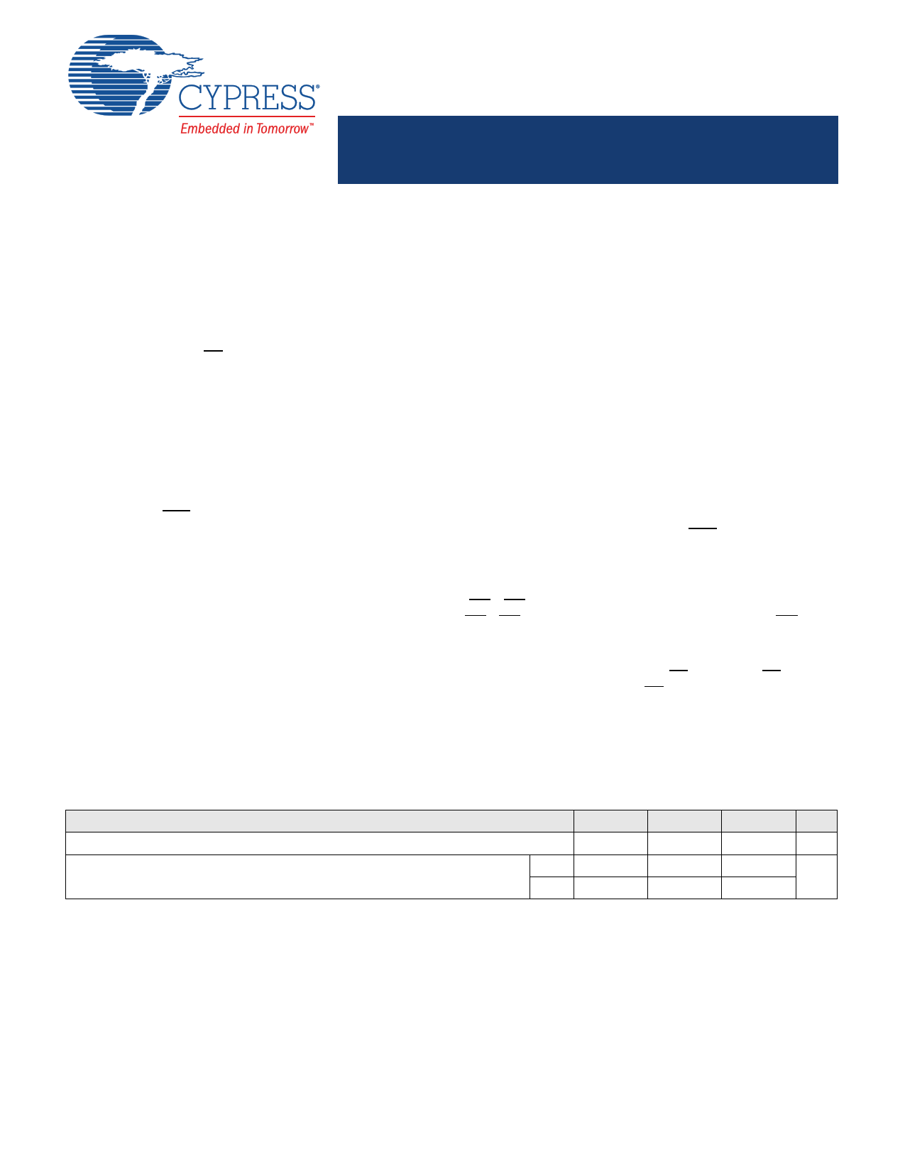
Selection Guide
Maximum access time
Maximum operating current
Description
250 MHz 200 MHz 167 MHz Unit
2.5 3.2 3.4 ns
× 18 220 190 170 mA
× 36 240 210 190
Cypress Semiconductor Corporation • 198 Champion Court
Document Number: 001-66680 Rev. *K
• San Jose, CA 95134-1709 • 408-943-2600
Revised July 5, 2016
1 page 
Pin Configurations
Figure 1. 100-pin TQFP Pinout
CY7C1460KV33
CY7C1460KVE33
CY7C1462KVE33
DQPc
DQc
DQc
VDDQ
VSS
DQc
DQc
DQc
DQc
VSS
VDDQ
DQc
DQc
NC
VDD
NC
VSS
DQd
DQd
VDDQ
VSS
DQd
DQd
DQd
DQd
VSS
VDDQ
DQd
DQd
DQPd
1
2
3
4
5
6
7
8
9
10
11
12
13
14 CY7C1460KV33/CY7C1460KVE33
15
16 (1M × 36)
17
18
19
20
21
22
23
24
25
26
27
28
29
30
80
79
78
77
76
75
74
73
72
71
70
69
68
67
66
65
64
63
62
61
60
59
58
57
56
55
54
53
52
51
DQPb NC
DQb
NC
DQb
VDDQ
VSS
DQb
DQb
NC
VDDQ
VSS
NC
NC
DQb DQb
DQb
VSS
VDDQ
DQb
DQb
VSS
VDDQ
DQb
DQb
VSS
NC
VDD
ZZ
DQa
DQb
NC
VDD
NC
VSS
DQb
DQa
VDDQ
VSS
DQa
DQb
VDDQ
VSS
DQb
DQa DQb
DQa DQPb
DQa NC
VSS
VDDQ
DQa
VVDSDSQ
NC
DQa NC
DQPa NC
1
2
3
4
5
6
7
8
9
10
11
12
13
14
15
16
17
18
19
20
21
22
23
24
25
26
27
28
29
30
CY7C1462KVE33
(2M × 18)
80 A
79 NC
78 NC
77 VDDQ
76 VSS
75 NC
74 DQPa
73 DQa
72 DQa
71 VSS
70 VDDQ
69 DQa
68 DQa
67 VSS
66 NC
65 VDD
64 ZZ
63 DQa
62 DQa
61 VDDQ
60 VSS
59 DQa
58 DQa
57 NC
56 NC
55 VSS
54 VDDQ
53 NC
52 NC
51 NC
Document Number: 001-66680 Rev. *K
Page 5 of 31
5 Page 
CY7C1460KV33
CY7C1460KVE33
CY7C1462KVE33
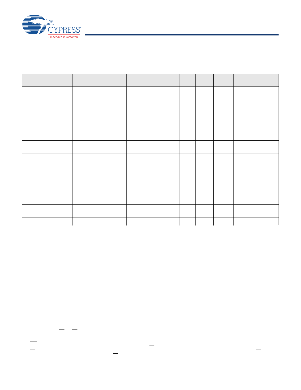
Truth Table
The Truth Table for CY7C1460KV33/CY7C1460KVE33/CY7C1462KVE33 follows. [1, 2, 3, 4, 5, 6, 7]
Operation
Address
Used
CE
ZZ ADV/LD WE BWx OE
CEN
Deselect cycle
None
HL
L
XX
X
L
Continue deselect cycle None
XL
H
XX
X
L
Read cycle
(begin burst)
Read cycle
(continue burst)
NOP/dummy read
(begin burst)
Dummy read
(continue burst)
Write cycle
(begin burst)
External L
L
L
HX
L
L
Next
XL
H
XX
L
L
External L
L
L
HX
H
L
Next
XL
H
XX
H
L
External L
L
L
LL X L
Write cycle
(continue burst)
Next
XL
H
XL X L
NOP/WRITE ABORT
(begin burst)
None
LL
L
LH
X
L
WRITE ABORT
(continue burst)
Next
XL
H
XH
X
L
IGNORE CLOCK EDGE
(stall)
Current
X
L
X
XX X H
SLEEP MODE
None
XH
X
XX
X
X
CLK
L–H
L-H
L–H
L–H
L–H
L–H
L–H
L–H
L–H
L–H
L–H
X
DQ
Tristate
Tristate
Data out (Q)
Data out (Q)
Tristate
Tristate
Data in (D)
Data in (D)
Tristate
Tristate
–
Tristate
Notes
1. X = “Don't Care”, H = Logic HIGH, L = Logic LOW, CE stands for all chip enables active. BWx = L signifies at least one byte write select is active, BWx = valid signifies
that the desired byte write selects are asserted, see Write Cycle Description table for details.
2. Write is defined by WE and BWX. See Write Cycle Description table for details.
3. When a write cycle is detected, all I/Os are tristated, even during byte writes.
4. The DQ and DQP pins are controlled by the current cycle and the OE signal.
5. CEN = H inserts wait states.
6. Device powers up deselected and the I/Os in a tristate condition, regardless of OE.
7. OE is asynchronous and is not sampled with the clock rise. It is masked internally during write cycles.During a read cycle DQs and DQPX = Tristate when OE is inactive
or when the device is deselected, and DQs=data when OE is active.
Document Number: 001-66680 Rev. *K
Page 11 of 31
11 Page | ||
| Páginas | Total 30 Páginas | |
| PDF Descargar | [ Datasheet CY7C1460KV33.PDF ] | |
Hoja de datos destacado
| Número de pieza | Descripción | Fabricantes |
| CY7C1460KV33 | 36-Mbit (1M x 36/2M x 18) Pipelined SRAM | Cypress Semiconductor |
| Número de pieza | Descripción | Fabricantes |
| SLA6805M | High Voltage 3 phase Motor Driver IC. |
Sanken |
| SDC1742 | 12- and 14-Bit Hybrid Synchro / Resolver-to-Digital Converters. |
Analog Devices |
|
DataSheet.es es una pagina web que funciona como un repositorio de manuales o hoja de datos de muchos de los productos más populares, |
| DataSheet.es | 2020 | Privacy Policy | Contacto | Buscar |
