|
|
|
PDF AD5821A Data sheet ( Hoja de datos )
| Número de pieza | AD5821A | |
| Descripción | I2C DAC | |
| Fabricantes | Analog Devices | |
| Logotipo | ||
Hay una vista previa y un enlace de descarga de AD5821A (archivo pdf) en la parte inferior de esta página. Total 16 Páginas | ||
|
No Preview Available !
FEATURES
Current sink: 120 mA
Available in 3 × 3 array WLCSP package
2-wire, (I2C-compatible) 1.8 V serial interface
10-bit resolution
Integrated current sense resistor
Power supply range: 2.7 V to 5.5 V
Guaranteed monotonic over all codes
Power down to 0.5 μA typical
Internal reference
Ultralow noise preamplifier
Power-down function
Power-on reset
APPLICATIONS
Consumer
Lens autofocus
Image stabilization
Optical zoom
Shutters
Iris/exposure
Neutral density (ND) filters
Lens covers
Camera phones
Digital still cameras
Camera modules
Digital video cameras/camcorders
Camera-enabled devices
Security cameras
Web/PC cameras
120 mA, Current Sinking,
10-Bit, I2C DAC
AD5821A
Industrial
Heater controls
Fan controls
Cooler (Peltier) controls
Solenoid controls
Valve controls
Linear actuator controls
Light controls
Current loop controls
GENERAL DESCRIPTION
The AD5821A is a single, 10-bit digital-to-analog converter
(DAC) with output current sinking capability of 120 mA. It
features an internal reference and operates from a single 2.7 V
to 5.5 V supply. The DAC is controlled via a 2-wire, I2C®-
compatible serial interface that operates at clock rates up to
400 kHz.
The AD5821A incorporates a power-on reset circuit that
ensures the DAC output powers up to 0 V and remains there until
a valid write takes place. It has a power-down feature that reduces
the current consumption of the device to 1 μA maximum.
The AD5821A is designed for autofocus, image stabilization,
and optical zoom applications in camera phones, digital still
cameras, and camcorders.
The AD5821A is also suitable for many industrial applications,
such as controlling temperature, light, and movement without
derating over temperatures ranging from −30°C to +85°C.
The I2C 7-bit address for the AD5821A is 0xC.
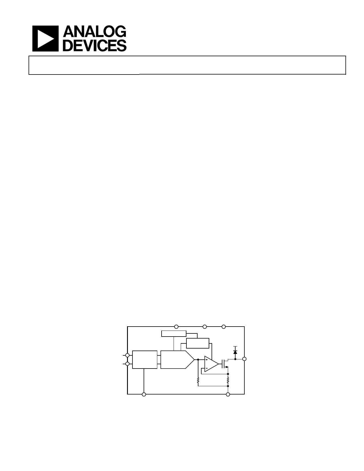
FUNCTIONAL BLOCK DIAGRAM
XSHUTDOWN
VDD
DGND
SDA
SCL
REFERENCE
POWER-ON
RESET
I2C SERIAL
INTERFACE
10-BIT
CURRENT
OUTPUT DAC
VDD
D1
ISINK
AD5821A
R
DGND
Figure 1.
RSENSE
3.3Ω
AGND
Rev. 0
Information furnished by Analog Devices is believed to be accurate and reliable. However, no
responsibility is assumed by Analog Devices for its use, nor for any infringements of patents or other
rights of third parties that may result from its use. Specifications subject to change without notice. No
license is granted by implication or otherwise under any patent or patent rights of Analog Devices.
Trademarksandregisteredtrademarksarethepropertyoftheirrespectiveowners.
One Technology Way, P.O. Box 9106, Norwood, MA 02062-9106, U.S.A.
Tel: 781.329.4700
www.analog.com
Fax: 781.461.3113
©2008 Analog Devices, Inc. All rights reserved.
1 page 
ABSOLUTE MAXIMUM RATINGS
TA = 25°C, unless otherwise noted.
Table 4.
Parameter
VDD to AGND
VDD to DGND
AGND to DGND
SCL, SDA to DGND
XSHUTDOWN to DGND
ISINK to AGND
Operating Temperature Range
Industrial (B Version)
Storage Temperature Range
Junction Temperature (TJ MAX)
WLCSP Power Dissipation
θJA Thermal Impedance1
Mounted on 4-Layer Board
Lead Temperature, Soldering
Maximum Peak Reflow Temperature2
Rating
−0.3 V to +5.5 V
−0.3 V to VDD + 0.3 V
−0.3 V to +0.3 V
−0.3 V to VDD + 0.3 V
−0.3 V to VDD + 0.3 V
−0.3 V to VDD + 0.3 V
−30°C to +85°C
−65°C to +150°C
150°C
(TJ MAX − TA)/θJA
95°C/W
260°C (±5°C)
1 To achieve the optimum θJA, it is recommended that the AD5821A be
soldered on a 4-layer board.
2 As per JEDEC J-STD-020C.
AD5821A
Stresses above those listed under Absolute Maximum Ratings
may cause permanent damage to the device. This is a stress
rating only; functional operation of the device at these or any
other conditions above those indicated in the operational
section of this specification is not implied. Exposure to absolute
maximum rating conditions for extended periods may affect
device reliability.
ESD CAUTION
Rev. 0 | Page 5 of 16
5 Page 
AD5821A
THEORY OF OPERATION
The AD5821A is a fully integrated, 10-bit DAC with 120 mA
output current sink capability. It is intended for driving voice
coil actuators in applications such as lens autofocus, image
stabilization, and optical zoom. The circuit diagram is shown in
Figure 20. A 10-bit current output DAC coupled with Resistor R
generates the voltage that drives the noninverting input of the
operational amplifier. This voltage also appears across the RSENSE
resistor and generates the sink current required to drive the
voice coil.
Resistor R and Resistor RSENSE are interleaved and matched.
Therefore, the temperature coefficient and any nonlinearities
over temperature are matched, and the output drift over tempera-
ture is minimized. Diode D1 is an output protection diode.
XSHUTDOWN
VDD DGND
SDA
SCL
REFERENCE
POWER-ON
RESET
I2C SERIAL
INTERFACE
10-BIT
CURRENT
OUTPUT DAC
VDD
D1
ISINK
AD5821A
R
RSENSE
3.3Ω
DGND
AGND
Figure 20. Block Diagram Showing Connection to Voice Coil
SERIAL INTERFACE
The AD5821A is controlled using the industry-standard I2C
2-wire serial protocol. Data can be written to or read from the
DAC at data rates of up to 400 kHz. After a read operation, the
contents of the input register are reset to all 0s.
I2C BUS OPERATION
An I2C bus operates with one or more master devices that
generate the serial clock (SCL) and read and write data on
the serial data line (SDA) to and from slave devices such as
the AD5821A. On all devices on an I2C bus, the SDA pin is
connected to the SDA line and the SCL pin connected to the
SCL line of the master device. I2C devices can only pull the bus
lines low; pulling high is achieved by pull-up resistors, RP. The
value of RP depends on the data rate, bus capacitance, and the
maximum load current that the I2C device can sink (3 mA for a
standard device).
1.8V
RP RP
SDA
SCL
When the bus is idle, SCL and SDA are both high. The master
device initiates a serial bus operation by generating a start
condition, which is defined as a high-to-low transition on the
SDA low while SCL is high. The slave device connected to the
bus responds to the start condition and shifts in the next eight
data bits under control of the serial clock.
These eight data bits consist of a 7-bit address, plus a read/write
(R/W) bit that is 0 if data is to be written to a device, and 1 if
data is to be read from a device. Each slave device on an I2C bus
must have a unique address. The address of the AD5821A is
0001100; however, 0001101, 0001110, and 0001111 address the
part because the last two bits are unused/don’t cares (see Figure 22
and Figure 23). Because the address plus the R/W bit always
equals eight bits of data, the write address of the AD5821A is
00011000 (0x18) and the read address is 00011001 (0x19) (see
Figure 22 and Figure 23).
At the end of the address data, after the R/W bit, the slave
device that recognizes its own address responds by generating
an acknowledge (ACK) condition. This is defined as the slave
device pulling SDA low while SCL is low before the ninth clock
pulse and keeping it low during the ninth clock pulse. Upon
receiving the ACK, the master device can clock data into the
AD5821A in a write operation, or it can clock it out in a read
operation. Data must change either during the low period of the
clock (because SDA transitions during the high period define a
start condition), or during a stop condition, as described in the
Data Format section.
I2C data is divided into blocks of eight bits, and the slave generates
an ACK at the end of each block. Because the AD5821A requires
10 bits of data, two data-words must be written to it when a
write operation occurs, or read from it when a read operation
occurs. At the end of a read or write operation, the AD5821A
acknowledges the second data byte. The master generates a stop
condition, defined as a low-to-high transition on SDA while SCL
is high, to end the transaction.
DATA FORMAT
Data is written to the AD5821A high byte first, MSB first, and is
shifted into the 16-bit input register. After all data is shifted in,
data from the input register is transferred to the DAC register.
Because the DAC requires only 10 bits of data, not all bits of the
input register data are used. The MSB is reserved for an active-
high, software-controlled, power-down function.
The data format is shown in Table 6. When referring to this table,
note that Bit 14 is unused; Bit 13 to Bit 4 correspond to the DAC
data bits, D9 to D0; and Bit 3 to Bit 0 are unused.
During a read operation, data is read in the same bit order.
I2C MASTER
DEVICE
I2C SLAVE
DEVICE
AD5821 A
Figure 21. Typical I2C Bus
I2C SLAVE
DEVICE
Rev. 0 | Page 11 of 16
11 Page | ||
| Páginas | Total 16 Páginas | |
| PDF Descargar | [ Datasheet AD5821A.PDF ] | |
Hoja de datos destacado
| Número de pieza | Descripción | Fabricantes |
| AD5821 | single 10-bit digital-to-analog converter | Analog Devices |
| AD5821A | I2C DAC | Analog Devices |
| Número de pieza | Descripción | Fabricantes |
| SLA6805M | High Voltage 3 phase Motor Driver IC. |
Sanken |
| SDC1742 | 12- and 14-Bit Hybrid Synchro / Resolver-to-Digital Converters. |
Analog Devices |
|
DataSheet.es es una pagina web que funciona como un repositorio de manuales o hoja de datos de muchos de los productos más populares, |
| DataSheet.es | 2020 | Privacy Policy | Contacto | Buscar |