|
|
|
PDF APL5546 Data sheet ( Hoja de datos )
| Número de pieza | APL5546 | |
| Descripción | Dual Channel 500mA/500mA Regulator + Reset IC | |
| Fabricantes | ANPEC | |
| Logotipo | ||
 1. Datasheet PDF - Dual-channel Regulator Hay una vista previa y un enlace de descarga de APL5546 (archivo pdf) en la parte inferior de esta página. Total 17 Páginas | ||
|
No Preview Available !
APL5546
Dual Channel 500mA/500mA Regulator + Reset IC
Features
General Description
• Low Quiescent Current : 110µA (No load)
• Low Dropout Voltage :
VDROP1=500mV@500mA
VDROP2=500mV@500mA
• Fixed Output Voltage :
VOUT1=3.3V/500mA
VOUT2=3.3V/500mA
• Stable with 4.7µF Output Capacitor
• Stable with Aluminum, Tantalum or Ceramic
Capacitors
• Built in Thermal Protection
• Fast Transient Response
• Short Setting Time
• SOP-8, SOP-8-P with Thermal Pad Packages
• Adjustment-free Reset Detection Voltage :
3.9V or 4.2V typ
• Easy to Set Delay Time from Voltage
Detection to Reset Release
Applications
• Optical Storage System
The APL5546 is a dual-channel regulator with reset
function (specific voltage monitoring), and internal de-
lay circuit, set to detect 3.9V or 4.2V. Maximum in-
put voltage is 6V, and both output1 and output2 can
deliver up to 500mA. The typical dropout voltage of
both channel is 500mV at 500mA loading. Design
with an internal P-channel MOSFET pass transistor,
the APL5546 maintains a low supply current. Other
features include, thermal-shutdown protection, current
limit protection to ensure specified output current. The
APL5546 come in miniature SOP-8 and SOP-8-P
packages.
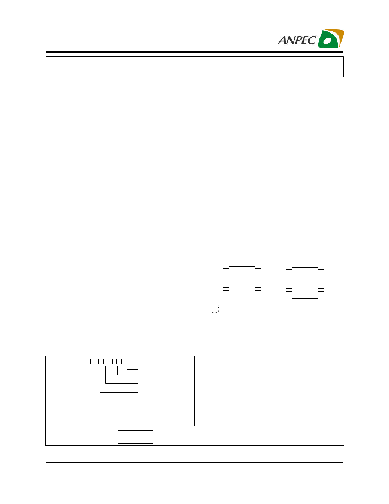
Pin Configuration
SOP-8 (Top View) SOP-8-P( Top View)
V IN
VOUT1
Cd
VDET
1
2
3
4
8 CONT
1V IN
7 GND
VOUT1
2
6 RESET Cd 3
5 VOUT2
VDET
4
8 CONT
7 GND
6 RESET
5 VOUT2
= Thermal Pad
(connected to GND plane for better heat
dissipation)
Ordering and Marking Information
APL5546 -
Lead Free Code
Handling Code
Temp. Range
Package Code
Detection Voltage
Package Code
K : SOP-8
KA : SOP-8-P
Temp. Range
C : 0 to 70°C I : -40 to 85°C
Handling Code
TR : Tape & Reel
Detection Voltage :
A : 3.9V
B : 4.2V
Lead Free Code
L : Lead Free Device
Blank : Original Device
APL5546 K / KA:
APL5546X
XXXXX
X - Detection Voltage
XXXXX - Date Code
ANPEC reserves the right to make changes to improve reliability or manufacturability without notice, and advise
customers to obtain the latest version of relevant information to verify before placing orders.
Copyright © ANPEC Electronics Corp.
Rev. A.3- Jul., 2006
1
www.anpec.com.tw
1 page 
APL5546
Application Circuit
1µF
RL
4.7kΩ
VIN VOUT1
VDET
APL5546
RESET
Cd
VOUT2
GND CONT
0.1µ F
3.3V
3.3V
COUT2
4.7µ F
COUT1
4.7µ F
Copyright © ANPEC Electronics Corp.
Rev. A.3 - Jul., 2006
5
www.anpec.com.tw
5 Page 
APL5546
Application Information
Capacitor Selection and Regulator Stabil-
ity
The APL5546 uses at least a 1uF capacitor on the
input. This capacitor can use Aluminum, Tantalum or
Ceramic capacitors. Input capacitor with large value
and low ESR provides better PSRR and line-transient
response. The output capacitor also can use
Aluminum, Tantalum or Ceramic capacitors, and it’s
minimum values is recommended 4.7uF, ESR muse
be above 0.01Ω. Large output capacitor values can
reduce noise and improve load-transient response,
stability, and PSRR. Note that some ceramic dielec-
trics exhibit large capacitance and ESR variation with
Temperature. If use this capacitor, it may be neces-
sary to use 4.7uF or more to ensure stability at tem-
perature below -10°C.
Load-Transient Considerations
The APL5546 load-transient response graphs in Typi-
cal Characteristics show the transient response. A
step change in the load current from 1mA to 500mA
at 1u second will cause less than 200mV transient
spike. Large output capacitor’s value and low ESR
can reduce transient spike.
RESET
The RESET pin is asserted whenever VDET falls below
the reset threshold voltage or if CONT is forced low at
some special IC(refer timing chart and pin description).
The reset function ensures the microprocessor is prop-
erly reset and powers up into a known condition after
a power failure. RESET will remain valid with VIN as
low as 0.95V. The RESET output is a simple open-
drain N channel MOSET structure. A pull-up resistor
must be used to pull this output up to some voltage.
For most application, this voltage will be the same
power supply that supplies VIN to the APL5546. The
APL5546 is relatively immune to negative-going
glitches below the reset threshold. Typically reset delay
time is 13ms while using 0.1uF at Cd pin. If more
transient immunity is needed, a Cd capacitor can be
placed as larger as possible.
Input-Output (Dropout)Voltage
The minimun input-output voltage differential (dropout)
determines the lowest usable supply voltage. The drop-
out voltage is a function of drain-to-source on resis-
tance multiplied by the load current.
Shutdown/Enable
The APL5546 has an active high enable function. Force
CONT high (>1.6V) enables the VOUT1 , CONT low (<0.
4V) disables the VOUT1 and VOUT2 can not be affected
by CONT. Enter the shutdown mode, it also causes
the output voltage to discharge through a 500 Ω resis-
tance to ground. In shutdown mode, the quiescent
current can reduce to 70uA. The CONT pin cannot be
floating, a floating CONT pin may cause an indetermi-
nate state on the output. If it is no use, connect to VIN
for normal operation.
Current Limit
APL5546 includes two separate current-limit circuitry
for each linear regulator. The current limit protection,
which sense the current flows the P-channel MOSFET,
and controls the output voltage. The point where limit-
ing occurs is IOUT=800mA. The output can be shorted
to ground for an indefinite amount of time without dam-
aging to the part.
Copyright © ANPEC Electronics Corp.
Rev. A.3 - Jul., 2006
11
www.anpec.com.tw
11 Page | ||
| Páginas | Total 17 Páginas | |
| PDF Descargar | [ Datasheet APL5546.PDF ] | |
Hoja de datos destacado
| Número de pieza | Descripción | Fabricantes |
| APL5546 | Dual Channel 500mA/500mA Regulator + Reset IC | ANPEC |
| Número de pieza | Descripción | Fabricantes |
| SLA6805M | High Voltage 3 phase Motor Driver IC. |
Sanken |
| SDC1742 | 12- and 14-Bit Hybrid Synchro / Resolver-to-Digital Converters. |
Analog Devices |
|
DataSheet.es es una pagina web que funciona como un repositorio de manuales o hoja de datos de muchos de los productos más populares, |
| DataSheet.es | 2020 | Privacy Policy | Contacto | Buscar |