|
|
|
PDF FQA11N90C_F109 Data sheet ( Hoja de datos )
| Número de pieza | FQA11N90C_F109 | |
| Descripción | MOSFET ( Transistor ) | |
| Fabricantes | Fairchild Semiconductor | |
| Logotipo | ||
Hay una vista previa y un enlace de descarga de FQA11N90C_F109 (archivo pdf) en la parte inferior de esta página. Total 9 Páginas | ||
|
No Preview Available !
FQA11N90C_F109
N-Channel QFET® MOSFET
900 V, 11.0 A, 1.1 Ω
Features
• 11 A, 900 V, RDS(on) = 1.1 Ω (Max.) @ VGS = 10 V, ID = 5.5 A
• Low Gate Charge (Typ. 60 nC)
• Low Crss (Typ. 23 pF)
• 100% Avalanche Tested
• RoHS compliant
April 2014
Description
This N-Channel enhancement mode power MOSFET is pro-
duced using Fairchild Semiconductor’s proprietary planar stripe
and DMOS technology. This advanced MOSFET technology
has been especially tailored to reduce on-state resistance, and
to provide superior switching performance and high avalanche
energy strength. These devices are suitable for switched mode
power supplies, active power factor correction (PFC), and elec-
tronic lamp ballasts.
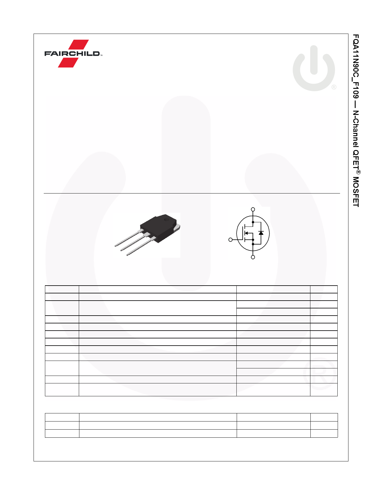
D
G
D
S
TO-3PN
G
MOSFET Maximum Ratings TC = 25oC unless otherwise noted.
Symbol
VDSS
ID
IDM
VGSS
EAS
IAR
EAR
dv/dt
PD
TJ, TSTG
TL
Parameter
Drain to Source Voltage
Drain Current
Drain Current
- Continuous (TC = 25oC)
- Continuous (TC = 100oC)
- Pulsed
Gate to Source Voltage
Single Pulsed Avalanche Energy
Avalanche Current
Repetitive Avalanche Energy
Peak Diode Recovery dv/dt
Power Dissipation
(TC = 25oC)
- Derate Above 25oC
Operating and Storage Temperature Range
Maximum Lead Temperature for Soldering,
1/8” from Case for 5 Seconds
(Note 1)
(Note 2)
(Note 1)
(Note 1)
(Note 3)
Thermal Characteristics
Symbol
RθJC
RθJA
Parameter
Thermal Resistance, Junction to Case, Max
Thermal Resistance, Junction to Ambient, Max
S
FQA11N90C_F109
900
11.0
6.9
44.0
± 30
960
11.0
30
4.0
300
2.38
-55 to +150
300
FQA11N90C_F109
0.42
40
Unit
V
A
A
A
V
mJ
A
mJ
V/ns
W
W/°C
°C
°C
Unit
oC/W
oC/W
©2006 Fairchild Semiconductor Corporation
FQA11N90C_F109 Rev. C2
1
www.fairchildsemi.com
1 page 
Figure 12. Gate Charge Test Circuit & Waveform
Same Type
50KΩ as DUT
12V 200nF
300nF
VGS
10V
VGS
VDS
Qgs
IG = co3nmsAt.
DUT
Qg
Qgd
Charge
V10GVS
Figure 13. Resistive Switching Test Circuit & Waveforms
VDS
VGS
RG
RL
VDD
DUT
VDS
90%
VGS 10%
td(on)
tr
t on
td(off)
tf
t off
V1G0GVSS
tp
Figure 14. Unclamped Inductive Switching Test Circuit & Waveforms
VDS
ID
RG
L
EAS = --21-- L IAS2
------B--V--D--S-S-------
BVDSS - VDD
BVDSS
IAS
VDD ID (t)
DUT
VDD
VDS (t)
t p Time
©2006 Fairchild Semiconductor Corporation
FQA11N90C_F109 Rev. C2
5
www.fairchildsemi.com
5 Page | ||
| Páginas | Total 9 Páginas | |
| PDF Descargar | [ Datasheet FQA11N90C_F109.PDF ] | |
Hoja de datos destacado
| Número de pieza | Descripción | Fabricantes |
| FQA11N90C_F109 | MOSFET ( Transistor ) | Fairchild Semiconductor |
| Número de pieza | Descripción | Fabricantes |
| SLA6805M | High Voltage 3 phase Motor Driver IC. |
Sanken |
| SDC1742 | 12- and 14-Bit Hybrid Synchro / Resolver-to-Digital Converters. |
Analog Devices |
|
DataSheet.es es una pagina web que funciona como un repositorio de manuales o hoja de datos de muchos de los productos más populares, |
| DataSheet.es | 2020 | Privacy Policy | Contacto | Buscar |