|
|
|
PDF 83058 Data sheet ( Hoja de datos )
| Número de pieza | 83058 | |
| Descripción | Single-Ended Multiplexer | |
| Fabricantes | IDT | |
| Logotipo | ||
Hay una vista previa y un enlace de descarga de 83058 (archivo pdf) en la parte inferior de esta página. Total 14 Páginas | ||
|
No Preview Available !
8:1, Single-Ended Multiplexer
83058
Datasheet
GENERAL DESCRIPTION
The 83058I is a low skew, 8:1, Single-ended Multiplexer
and a member of the family of High Performance Clock
Solutions from IDT. The 83058I has eight selectable single-
ended clock inputs and one single-ended clock output. The
output has a V pin which may be set at 3.3V, 2.5V, or
DDO
1.8V, making the device ideal for use in voltage transla-
tion applications. An output enable pin places the output in
a high impedance state which may be useful for testing or
debug purposes. The device operates up to 250MHz and is pack-
aged in a 16 TSSOP package.
FEATURES
• 8:1 single-ended multiplexer
• Q nominal output impedance: 7Ω (V = 3.3V)
DDO
• Maximum output frequency: 250MHz
• Propagation delay: 3ns (maximum), V = V = 3.3V
DD DDO
• Input skew: 225ps (maximum), V = V = 3.3V
DD DDO
• Part-to-part skew: 475ps (maximum), V = V = 3.3V
DD DDO
• Additive phase jitter, RMS: 0.19ps (typical), 3.3V/3.3V
• Operating supply modes:
V /V
DD DDO
3.3V/3.3V
3.3V/2.5V
3.3V/1.8V
2.5V/2.5V
2.5V/1.8V
• -40°C to 85°C ambient operating temperature
• Available in lead-free (RoHS 6) package
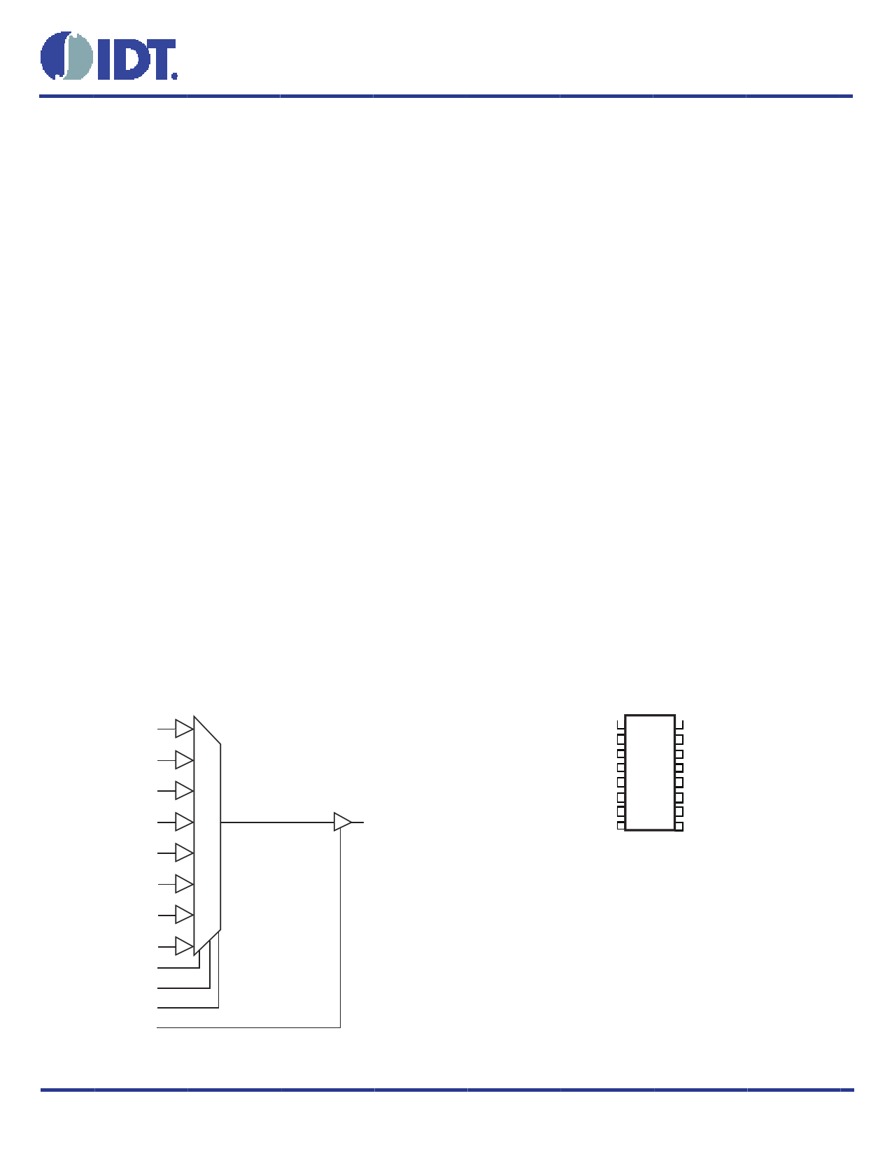
BLOCK DIAGRAM
CLK0
CLK1
CLK2
CLK3
CLK4
CLK5
CLK6
CLK7
SEL2
SEL1
SEL0
OE
©2015 Integrated Device Technology, Inc
PIN ASSIGNMENT
Q1
16 VDDO
CLK7 2
15 CLK0
OE 3
14 SEL0
CLK6 4
13 CLK1
GND 5
12 VDD
CLK5 6
11 CLK2
SEL2 7
10 SEL1
Q
CLK4 8
9 CLK3
83058I
16-Lead TSSOP
4.4mm x 5.0mm x 0.92mm package body
G Package
Top View
1 December 15, 2015
1 page 
83058 Datasheet
TABLE 5B. AC CHARACTERISTICS, V = 3.3V ± 5%, V = 2.5V ± 5%, TA = -40°C TO 85°C
DD DDO
Symbol Parameter
Test Conditions
Minimum Typical Maximum
f
MAX
tp
LH
tp
HL
tsk(i)
Output Frequency
Propagation Delay, Low to High; NOTE 1
Propagation Delay, High to Low; NOTE 1
Input Skew; NOTE 2
250
2.0 2.5 3.1
2.6 2.8 3.0
45 150
Buffer Additive Phase Jitter, RMS;
tjit refer to Additive Phase Jitter Section;
NOTE 3
155.52MHz,
(12kHz to 20MHz)
0.14
tsk(pp) Part-to-Part Skew; NOTE 2, 4
400
t /t
RF
odc
Output Rise/Fall Time
Output Duty Cycle
20% to 80%
50
45
500
55
MUX MUX Isolation
ISOL
@ 100MHz
45
NOTE 1: Measured from V /2 of the input to V /2 of the output.
DD DDO
NOTE 2: This parameter is defined in accordance with JEDEC Standard 65.
NOTE 3: Driving only one input clock.
NOTE 4: Defined as skew between outputs on different devices operating a the same supply voltages and
with equal load conditions. Using the same type of input on each device, the output is measured at V /2.
DDO
Units
MHz
ns
ns
ps
ps
ps
ps
%
dB
TABLE 5C. AC CHARACTERISTICS, V = 3.3V ± 5%, V = 1.8V ± 5%, TA = -40°C TO 85°C
DD DDO
Symbol Parameter
Test Conditions
Minimum Typical Maximum
f
MAX
tp
LH
tp
HL
tsk(i)
Output Frequency
Propagation Delay, Low to High; NOTE 1
Propagation Delay, High to Low; NOTE 1
Input Skew; NOTE 2
250
2.3 2.9 3.8
2.8 3.3 3.8
50 150
Buffer Additive Phase Jitter, RMS;
tjit refer to Additive Phase Jitter Section;
NOTE 3
155.52MHz,
(12kHz to 20MHz)
0.16
tsk(pp) Part-to-Part Skew; NOTE 2, 4
475
t /t
RF
odc
Output Rise/Fall Time
Output Duty Cycle
20% to 80%
100
45
700
55
MUX MUX Isolation
ISOL
@ 100MHz
45
NOTE 1: Measured from V /2 of the input to V /2 of the output.
DD DDO
NOTE 2: This parameter is defined in accordance with JEDEC Standard 65.
NOTE 3: Driving only one input clock.
NOTE 4: Defined as skew between outputs on different devices operating a the same supply voltages and
with equal load conditions. Using the same type of input on each device, the output is measured at V /2.
DDO
Units
MHz
ns
ns
ps
ps
ps
ps
%
dB
©2015 Integrated Device Technology, Inc
5
December 15, 2015
5 Page 
RELIABILITY INFORMATION
83058 Datasheet
TABLE 6. θ VS. AIR FLOW TABLE FOR 16 LEAD TSSOP
JA
θJA by Velocity (Linear Feet per Minute)
Single-Layer PCB, JEDEC Standard Test Boards
Multi-Layer PCB, JEDEC Standard Test Boards
0
137.1°C/W
89.0°C/W
200
118.2°C/W
81.8°C/W
500
106.8°C/W
78.1°C/W
NOTE: Most modern PCB designs use multi-layered boards. The data in the second row pertains to most designs.
TRANSISTOR COUNT
The transistor count for 83058I is: 874
PACKAGE OUTLINE AND PACKAGE DIMENSIONS
PACKAGE OUTLINE - G SUFFIX FOR 16 LEAD TSSOP
TABLE 7. PACKAGE DIMENSIONS
SYMBOL
Millimeters
Minimum
Maximum
N 16
A -- 1.20
A1 0.05 0.15
A2 0.80 1.05
b 0.19 0.30
c 0.09 0.20
D 4.90 5.10
E 6.40 BASIC
E1 4.30 4.50
e 0.65 BASIC
L 0.45 0.75
α 0° 8°
aaa -- 0.10
Reference Document: JEDEC Publication 95, MO-153
©2015 Integrated Device Technology, Inc
11
December 15, 2015
11 Page | ||
| Páginas | Total 14 Páginas | |
| PDF Descargar | [ Datasheet 83058.PDF ] | |
Hoja de datos destacado
| Número de pieza | Descripción | Fabricantes |
| 8305 | Connector Modules with Intergrated LAN Magnetics | ETC |
| 83054 | Single-Ended Multiplexer | IDT |
| 83056 | Single-Ended Multiplexer | IDT |
| 83058 | Single-Ended Multiplexer | IDT |
| Número de pieza | Descripción | Fabricantes |
| SLA6805M | High Voltage 3 phase Motor Driver IC. |
Sanken |
| SDC1742 | 12- and 14-Bit Hybrid Synchro / Resolver-to-Digital Converters. |
Analog Devices |
|
DataSheet.es es una pagina web que funciona como un repositorio de manuales o hoja de datos de muchos de los productos más populares, |
| DataSheet.es | 2020 | Privacy Policy | Contacto | Buscar |