|
|
|
PDF DS1682 Data sheet ( Hoja de datos )
| Número de pieza | DS1682 | |
| Descripción | Total-Elapsed-Time Recorder | |
| Fabricantes | Maxim Integrated | |
| Logotipo | ||
Hay una vista previa y un enlace de descarga de DS1682 (archivo pdf) en la parte inferior de esta página. Total 14 Páginas | ||
|
No Preview Available !
DS1682
Total-Elapsed-Time Recorder
with Alarm
General Description
The DS1682 is an integrated elapsed-time recorder con-
taining a factory-calibrated, temperature-compensated
RC time base that eliminates the need for an external
crystal. Using EEPROM technology to maintain data in
the absence of power, the DS1682 requires no backup
power source. The DS1682 detects and records the num-
ber of events on the EVENT pin and the total cumulative
event time since the DS1682 was last reset to 0. The
ALARM pin alerts the user when the total time accu-
mulated equals the user-programmed alarm value. The
polarity of the open-drain ALARM pin can be programmed
to either drive low or to become high impedance upon an
alarm condition. The DS1682 is ideal for applications that
monitor the total amount of time that a device has been
in operation and/or the number of uses since inception of
service, repair, or the last calibration.
Applications
●● High-Temp, Rugged, Industrial Applications Where
Vibration or Shock Could Damage a Quartz Crystal
●● Any System Where Time-of-Use is Important
(Warranty Tracking)
For related parts and recommended products to use with this part, refer
to www.maximintegrated.com/DS1682.related.
Benefits and Features
●● Records the Total Time That the Event Input Has
Been Active and the Number of Events That Have
Occurred
●● 32-Bit, Nonvolatile, Elapsed Time Counter (ETC)
Monitors Event Duration with Quarter-Second
Resolution and Provides 34 Years of Total Time
Accumulation
●● Programmable Elapsed Time ALARM Output
●● Nonvolatile, 17-Bit Event Counter Records the Total
Number of Times an Event has Occurred
●● Calibrated, Temperature-Compensated RC Time
Base Accurate to 2% Typical
●● 10 Bytes of EEPROM User Memory
●● Write Disable Function to Prevent the Memory from
Being Changed or Erased
●● 2-Wire Serial Communication
●● Wide 2.5V to 5.5V Power-Supply Range
●● Useful in Time-of-Use Warranty, Calibration, Repair,
and Maintenance Applications
Ordering Information appears at end of data sheet.
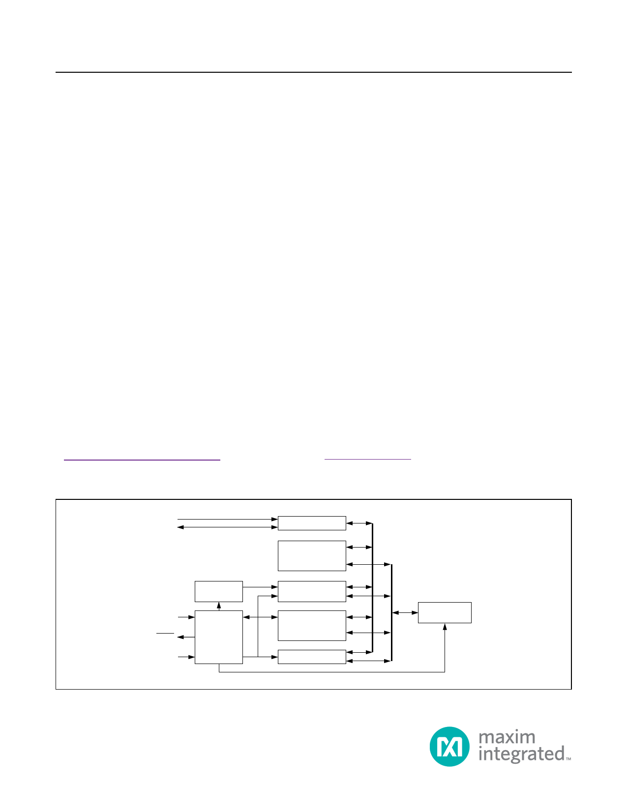
SCL
SDA
DS1682
VCC
ALARM
EVENT
OSCILLATOR
AND DIVIDER
CONTROL
LOGIC AND
EVENT
GLITCH
FILTER
Figure 1. Block Diagram
SERIAL INTERFACE
USER, CONTROL, AND
CONFIGURATION
REGISTERS
ELAPSED TIME
COUNTER (ETC)
ALARM REGS
AND
COMPARE LOGIC
EVENT COUNTER
EEPROM ARRAY
19-6835; Rev 1; 11/13
1 page 
DS1682
Pin Configuration
Total-Elapsed-Time Recorder
with Alarm
TOP VIEW
EVENT 1
+
N.C. 2
DS1682
ALARM 3
GND 4
SO
(150 mils)
8 VCC
7 N.C.
6 SDA
5 SCL
Pin Description
PIN NAME
FUNCTION
Event Input. The EVENT pin is the input the DS1682 monitors to determine when an event occurs. When
the pin is pulled high, the contents of the EEPROM are transferred to the ETC and the oscillator starts.
The ETC begins to count in quarter-second increments. When the EVENT pin falls to logic 0, the event
1 EVENT counter increments, and the event counter, ETC, and user-memory data are stored in the EEPROM array.
When the EVENT pin changes states, the 2-wire bus is unavailable for communications for tEW (falling)
and tER (rising). The EVENT input is also deglitched (tG) to prevent short noise spikes from triggering an
event.
2, 7 N.C. No Connection. These pins are not connected internally.
Active-Low Alarm Output. The DS1682 monitors the values in the ETC for the programmed value in
3
ALARM
the alarm register. When the ETC matches the alarm value, the alarm flag (AF) is set. Once set, the
alarm flag cannot be reset. See the operating descriptions for the AOS and AP bits for details about the
operation of the ALARM pin.
4 GND Ground
5
SCL
2-Wire Serial-Clock Input. The SCL pin is the serial-clock input for the 2-wire synchronous
communications channel. The SCL pin is an input that requires an external pullup resistor.
6
SDA
2-Wire Input/Output. The SDA pin is the data input/output signal for the 2-wire synchronous
communications channel. The SDA pin is an open-drain I/O, which requires an external pullup resistor.
8 VCC +2.5V to +5.5V Input Supply
www.maximintegrated.com
Maxim Integrated │ 5
5 Page 
DS1682
Total-Elapsed-Time Recorder
with Alarm
User Memory
There are 10 bytes of user-programmable, EEPROM
memory. Once the write-memory disable flag is set to
1, the memory becomes read-only. User memory is not
stored in EEPROM until an event becomes inactive.
2-Wire Serial Data Bus
The DS1682 supports a bidirectional, 2-wire bus and
data-transmission protocol. A device that sends data onto
the bus is defined as a transmitter and a device receiving
data, a receiver. The device that controls the message is
called a master, and the devices controlled by the master
are slaves. A master device that generates the serial clock
(SCL), controls the bus access, and generates the START
and STOP conditions must control the bus. The DS1682
operates as a slave on the 2-wire bus. Connections to
the bus are made through the open-drain I/O lines SDA
and SCL.
The following bus protocol has been defined (Figure 6):
●● Data transfer can be initiated only when the bus is
not busy.
●● During data transfer, the data line must remain stable
whenever the clock line is high. Changes in the data
line while the clock line is high are interpreted as
control signals.
Accordingly, the following bus conditions have been
defined:
Bus Not Busy: Both data and clock lines remain high.
Start Data Transfer: A change in the state of the data
line, from high to low, while the clock is high,
defines a START condition.
Stop Data Transfer: A change in the state of the data
line, from low to high, while the clock line is high, defines
the STOP condition.
Data Valid: The state of the data line represents valid
data when, after a START condition, the data line is stable
for the duration of the high period of the clock signal. The
data on the line must be changed during the low period of
the clock signal. There is one clock pulse per bit of data.
Each data transfer is initiated with a START condition
and terminated with a STOP condition. The number of
data bytes transferred between START and STOP condi-
tions are not limited, and are determined by the master
device. The information is transferred byte-wise and each
receiver acknowledges with a ninth bit. Within the bus
specifications a standard mode (100kHz clock rate) and a
fast mode (400kHz clock rate) are defined.
Acknowledge: Each receiving device, when addressed,
is obliged to generate an acknowledge after it receives
each byte. The master device must generate an extra
clock pulse, which is associated with this acknowledge bit.
A device that acknowledges must pull down the SDA line
during the acknowledge clock pulse in such a way that
the SDA line is stable low during the high period of the
acknowledge-related clock pulse. Of course, setup and
hold times must be considered. A master must signal an
end-of-data to the slave by not generating an acknowl-
edge bit on the last byte that has been clocked out of the
slave. In this case, the slave must leave the data line high
to enable the master to generate the STOP condition.
SDA
SCL
START
CONDITION
MSB SLAVE ADDRESS
12
6
R/W
DIRECTION
BIT
ACKNOWLEDGEMENT
SIGNAL FROM RECEIVER
ACKNOWLEDGEMENT
SIGNAL FROM RECEIVER
78 9
ACK
1 2 3-8 8 9
ACK
REPEATED IF MORE BYTES
ARE TRANSFERRED
STOP CONDITION
OR
REPEATED
START CONDITION
Figure 6. Timing Diagram: Data Transfer on 2-Wire Serial Bus
www.maximintegrated.com
Maxim Integrated │ 11
11 Page | ||
| Páginas | Total 14 Páginas | |
| PDF Descargar | [ Datasheet DS1682.PDF ] | |
Hoja de datos destacado
| Número de pieza | Descripción | Fabricantes |
| DS1680 | Portable System Controller | Dallas Semiconductor |
| DS1682 | Total-Elapsed-Time Recorder | Maxim Integrated |
| DS1682 | Total Elapsed Time Recorder | Dallas Semiconductor |
| DS1683 | Total-Elapsed-Time and Event Recorder | Maxim Integrated |
| Número de pieza | Descripción | Fabricantes |
| SLA6805M | High Voltage 3 phase Motor Driver IC. |
Sanken |
| SDC1742 | 12- and 14-Bit Hybrid Synchro / Resolver-to-Digital Converters. |
Analog Devices |
|
DataSheet.es es una pagina web que funciona como un repositorio de manuales o hoja de datos de muchos de los productos más populares, |
| DataSheet.es | 2020 | Privacy Policy | Contacto | Buscar |