|
|
|
PDF 9ZX21901C Data sheet ( Hoja de datos )
| Número de pieza | 9ZX21901C | |
| Descripción | 19-Output Differential Zbuffer | |
| Fabricantes | IDT | |
| Logotipo | ||
Hay una vista previa y un enlace de descarga de 9ZX21901C (archivo pdf) en la parte inferior de esta página. Total 20 Páginas | ||
|
No Preview Available !
19-Output Differential Zbuffer for PCIe Gen2/3
and QPI
9ZX21901C
DATASHEET
General Description
The 9ZX21901 is Intel DB1900Z Differential Buffer suitable for
PCI-Express Gen3 or QPI applications. The part is backwards
compatible to PCIe Gen1 and Gen2. A fixed external feedback
maintains low drift for critical QPI applications. In bypass
mode, the 9ZX21901 can provide outputs up to 400MHz.
Recommended Application
• 19-output PCIe Gen3/QPI buffer with fixed feedback for
Romley platforms
Output Features
• 19 – 0.7V current mode differential HCSL output pairs
Key Specifications
• Cycle-to-cycle jitter: < 50ps
• Output-to-output skew: <65ps
• Input-to-output delay: Fixed at 0 ps
• Input-to-output delay variation: <50ps
• Phase jitter: PCIe Gen3 < 1ps rms
• Phase jitter: QPI 9.6GB/s < 0.2ps rms
Features/Benefits
• Fixed feedback path/ 0ps input-to-output delay
• 9 Selectable SMBus addresses; Multiple devices can share
same SMBus segment
• 8 dedicated OE# pins; hardware control of outputs
• PLL or bypass mode; PLL can dejitter incoming clock
• Selectable PLL BW; minimizes jitter peaking in downstream
PLL's
• Spread spectrum compatible; tracks spreading input clock
for EMI reduction
• SMBus Interface; unused outputs can be disabled
• 100MHz & 133.33MHz PLL mode; legacy QPI support
• Undriven differential outputs in Power Down mode for
maximum power savings
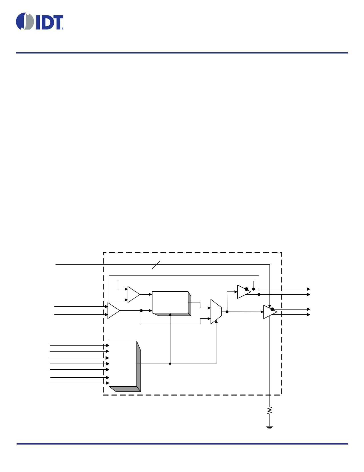
Functional Block Diagram
OE(12:5)#
8
DIF_IN
DIF_IN#
Z-PLL
(SS
Compatible)
Bypass path
HIBW_BYPM_LOBW#
100M_133M#
CKPWRGD/PD#
SMB_A0_tri
SMB_A1_tri
SMBDAT
SMBCLK
Logic
Note: Even though the feedback is fixed, DFB_OUT still
needs a termination network for the part to function.
9ZX21901C REVISION N 11/19/15
1
DFB_OUT
DIF(18:0)
IREF
©2015 Integrated Device Technology, Inc.
1 page 
9ZX21901C DATASHEET
Electrical Characteristics – Absolute Maximum Ratings
PARAMETER
SYMBOL
CONDITIONS
3.3V Core Supply Voltage VDDA
3.3V Logic Supply Voltage VDD
Input Low Voltage
VIL
Input High Voltage
VIH
Except for SMBus interface
Input High Voltage
VIHSMB
SMBus clock and data pins
Storage Temperature
Ts
Junction Temperature
Tj
Case Temperature
Tc
Input ESD protection ESD prot
Human Body Model
1Guaranteed by design and characterization, not 100% tested in production.
2 Operation under these conditions is neither implied nor guaranteed.
MIN
GND-0.5
-65
2000
TYP
MAX
4.6
4.6
VDD+0.5V
5.5V
150
125
110
UNITS
V
V
V
V
V
°C
°C
°C
V
NOTES
1,2
1,2
1
1
1
1
1
1
1
Electrical Characteristics – DIF_IN Clock Input Parameters
TAMB=TCOM unless otherwise indicated, Supply Voltages per normal operation conditions, See Test Loads for Loading Conditions
PARAMETER
SYMBOL
CONDITIONS
MIN
TYP
MAX UNITS NOTES
Input Crossover Voltage -
DIF_IN
Input Swing - DIF_IN
Input Slew Rate - DIF_IN
VCROSS
VSWING
dv/dt
Cross Over Voltage
Differential value
Measured differentially
150 900 mV 1
300 mV 1
0.4 8 V/ns 1,2
Input Leakage Current
Input Duty Cycle
IIN
dtin
VIN = VDD , VIN = GND
Measurement from differential wavefrom
-5
45
5 uA
55 % 1
Input Jitter - Cycle to Cycle JDIFIn
Differential Measurement
1 Guaranteed by design and characterization, not 100% tested in production.
2Slew rate measured through +/-75mV window centered around differential zero
0
125 ps 1
Electrical Characteristics – Current Consumption
TA = TCOM; Supply Voltage VDD/VDDA = 3.3 V +/-5%, See Test Loads for Loading Conditions
PARAMETER
SYMBOL
CONDITIONS
MIN
Operating Supply Current IDD3.3OP All outputs active @100MHz, CL = Full load;
Powerdown Current
IDD3.3PDZ
All differential pairs tri-stated
1Guaranteed by design and characterization, not 100% tested in production.
TYP MAX UNITS
407 500 mA
12 36 mA
NOTES
1
1
REVISION N 11/19/15
5 19-OUTPUT DIFFERENTIAL ZBUFFER FOR PCIE GEN2/3 AND QPI
5 Page 
9ZX21901C DATASHEET
General SMBus Serial Interface Information
(see also 9ZX21901 SMBus Addressing on page 2)
How to Write
• Controller (host) sends a start bit
• Controller (host) sends the write address XX(H)
• IDT clock will acknowledge
• Controller (host) sends the beginning byte location = N
• IDT clock will acknowledge
• Controller (host) sends the byte count = X
• IDT clock will acknowledge
• Controller (host) starts sending Byte N through Byte
N+X-1
• IDT clock will acknowledge each byte one at a time
• Controller (host) sends a Stop bit
Index Block Write Operation
Controller (Host)
IDT (Slave/Receiver)
T starT bit
Slave Address
WR WRite
ACK
Beginning Byte = N
ACK
Data Byte Count = X
ACK
Beginning Byte N
ACK
O
OO
OO
O
Byte N + X - 1
ACK
P stoP bit
Note: XX(H) is defined by SMBus Address select pins.
How to Read
• Controller (host) will send a start bit
• Controller (host) sends the write address XX(H)
• IDT clock will acknowledge
• Controller (host) sends the beginning byte location = N
• IDT clock will acknowledge
• Controller (host) will send a separate start bit
• Controller (host) sends the read address YY(H)
• IDT clock will acknowledge
• IDT clock will send the data byte count = X
• IDT clock sends Byte N+X-1
• IDT clock sends Byte 0 through Byte X (if X(H) was
written to Byte 8)
• Controller (host) will need to acknowledge each byte
• Controller (host) will send a not acknowledge bit
• Controller (host) will send a stop bit
Index Block Read Operation
Controller (Host)
T starT bit
IDT (Slave/Receiver)
Slave Address
WR WRite
ACK
Beginning Byte = N
ACK
RT Repeat starT
Slave Address
RD ReaD
ACK
ACK
ACK
O
O
O
N Not acknowledge
P stoP bit
Data Byte Count=X
Beginning Byte N
O
O
O
Byte N + X - 1
REVISION N 11/19/15
11 19-OUTPUT DIFFERENTIAL ZBUFFER FOR PCIE GEN2/3 AND QPI
11 Page | ||
| Páginas | Total 20 Páginas | |
| PDF Descargar | [ Datasheet 9ZX21901C.PDF ] | |
Hoja de datos destacado
| Número de pieza | Descripción | Fabricantes |
| 9ZX21901B | 19-Output Differential Zbuffer | IDT |
| 9ZX21901C | 19-Output Differential Zbuffer | IDT |
| Número de pieza | Descripción | Fabricantes |
| SLA6805M | High Voltage 3 phase Motor Driver IC. |
Sanken |
| SDC1742 | 12- and 14-Bit Hybrid Synchro / Resolver-to-Digital Converters. |
Analog Devices |
|
DataSheet.es es una pagina web que funciona como un repositorio de manuales o hoja de datos de muchos de los productos más populares, |
| DataSheet.es | 2020 | Privacy Policy | Contacto | Buscar |