|
|
|
PDF 854S006I Data sheet ( Hoja de datos )
| Número de pieza | 854S006I | |
| Descripción | Differential-to-LVDS Fanout Buffer | |
| Fabricantes | IDT | |
| Logotipo | ||
Hay una vista previa y un enlace de descarga de 854S006I (archivo pdf) en la parte inferior de esta página. Total 15 Páginas | ||
|
No Preview Available !
Low Skew, 1-to-6, Differential-to-
LVDS Fanout Buffer
854S006I
Data Sheet
GENERAL DESCRIPTION
The 854S006I is a low skew, high perfor- mance 1-to-6 Differen-
tial-to-LVDS Fanout Buffer. The CLK, nCLK pair can accept most
standard differential input levels. The 854S006I is characterized
to operate from either a 2.5V or a 3.3V power supply. Guaranteed
output skew characteristics make the 854S006I ideal for those clock
distribution applications demanding well defined performance and
repeatability.
FEATURES
• Six differential LVDS outputs
• One differential clock input pair
• CLK, nCLK pair can accept the following differential
input levels: LVDS, LVPECL, LVHSTL, SSTL, HCSL
• Maximum output frequency: 1.7GHz
• Translates any single ended input signal to LVDS levels
with resistor bias on nCLK input
• Output skew: 55ps (maximum)
• Propagation delay: 850ps (maximum)
• Additive phase jitter, RMS: 0.067ps (typical)
• Full 3.3V or 2.5V power supply
• -40°C to 85°C ambient operating temperature
• Available in lead-free (RoHS 6) packages
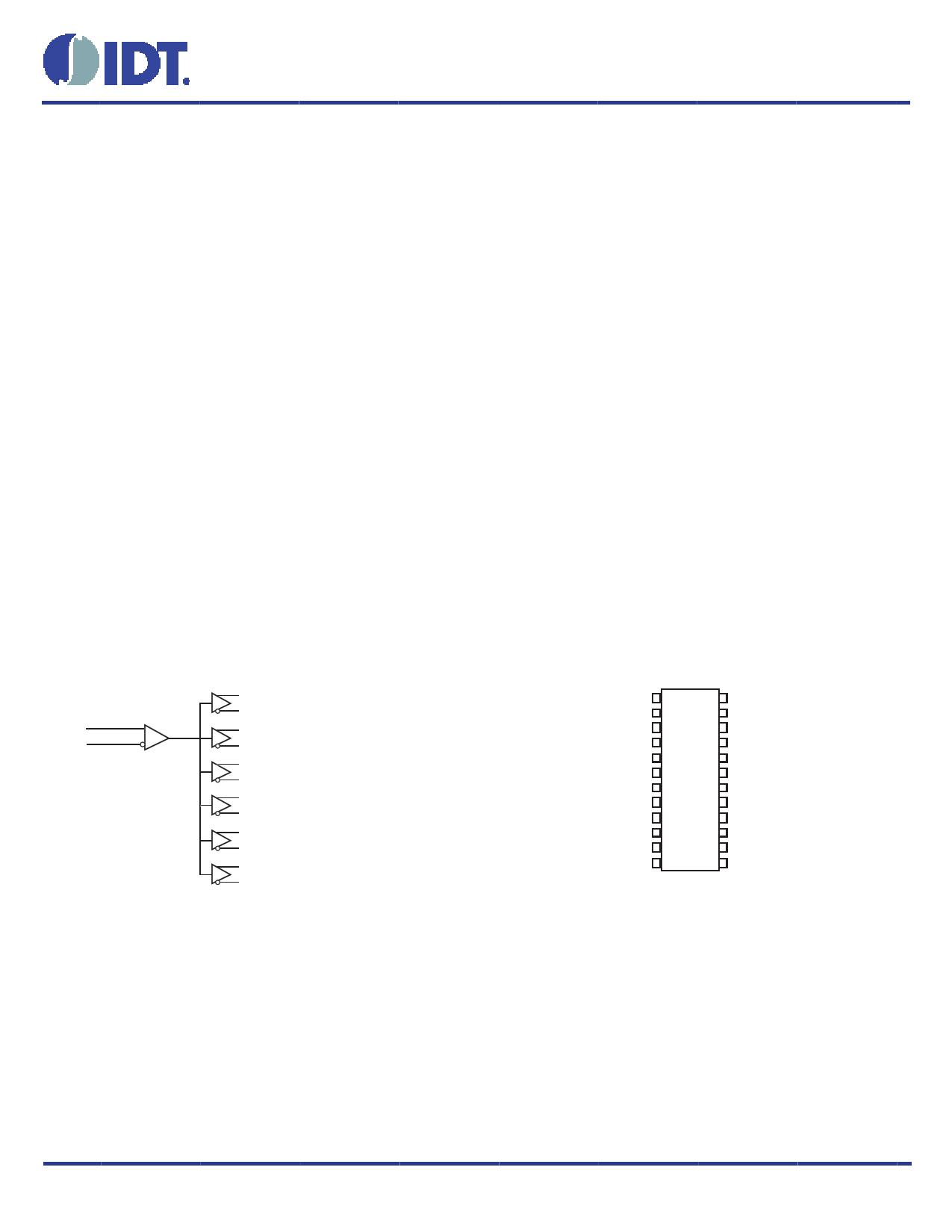
BLOCK DIAGRAM
CLK Pullup
nCLK Pulldown
Q0
nQ0
Q1
nQ1
Q2
nQ2
Q3
nQ3
Q4
nQ4
Q5
nQ5
PIN ASSIGNMENT
nCLK
CLK
VDD
VDDO
Q0
nQ0
GND
Q1
nQ1
VDDO
Q2
nQ2
1
2
3
4
5
6
7
8
9
10
11
12
24 GND
23 GND
22 VDD
21 VDDO
20 nQ5
19 Q5
18 GND
17 nQ4
16 Q4
15 VDDO
14 nQ3
13 Q3
854S006I
24-Lead TSSOP
4.40mm x 7.8mm x 0.925mm package body
G Package
Top View
©2016 Integrated Device Technology, Inc
1
Revision B January 19, 2016
1 page 
854S006I Data Sheet
ADDITIVE PHASE JITTER
The spectral purity in a band at a specific offset from the fundamental
compared to the power of the fundamental is called the dBc Phase
Noise. This value is normally expressed using a Phase noise plot
and is most often the specified plot in many applications. Phase
noise is defined as the ratio of the noise power present in a 1Hz
band at a specified offset from the fundamental frequency to the
power value of the fundamental. This ratio is expressed in decibels
(dBm) or a ratio of the power in the 1Hz band to the power in the
fundamental. When the required offset is specified, the phase noise
is called a dBc value, which simply means dBm at a specified offset
from the fundamental. By investigating jitter in the frequency domain,
we get a better understanding of its effects on the desired application
over the entire time record of the signal. It is mathematically possible
to calculate an expected bit error rate given a phase noise plot.
Input/Output Additive Phase Jitter @
622.08MHz (12kHz to 20MHz)
= 0.067ps (typical)
OFFSET FROM CARRIER FREQUENCY (HZ)
As with most timing specifications, phase noise measurements has
issues relating to the limitations of the equipment. Often the noise
floor of the equipment is higher than the noise floor of the device.
This is illustrated above. The device meets the noise floor of what
is shown, but can actually be lower. The phase noise is dependent
on the input source and measurement equipment.
©2016 Integrated Device Technology, Inc
5
Revision B January 19, 2016
5 Page 
854S006I Data Sheet
POWER CONSIDERATIONS
This section provides information on power dissipation and junction temperature for the 854S006I.
Equations and example calculations are also provided.
1. Power Dissipation.
The total power dissipation for the 854S006I is the sum of the core power plus the power dissipated in the load(s).
The following is the power dissipation for V = 3.3V + 5% = 3.465V, which gives worst case results.
DD
• Power (core) = V * I = 3.465V * 55mA = 190.575mW
MAX
DD_MAX
DD_MAX
• Power (outputs) = V * I = 3.465V * 105mA = 363.825mW
MAX
DDO_MAX DDO_MAX
Total Power = 190.575mW + 363.825mW = 554.4mW
_MAX
2. Junction Temperature.
Junction temperature at the junction of the bond wire and bond pad directly affects the reliability of the device. The maximum
recommended junction temperature is 125°C. Limiting the internal transistor junction temperature, Tj, to 125°C ensures that the
bond wire and bond pad temperature remains below 125°C.
The equation for Tj is as follows: Tj = θJA * Pd_total + TA
Tj = Junction Temperature
θJA = Junction-to-Ambient Thermal Resistance
Pd_total = Total Device Power Dissipation (example calculation is in section 1 above)
TA = Ambient Temperature
In order to calculate junction temperature, the appropriate junction-to-ambient thermal resistance θJA must be used. Assuming
no air flow and a multi-layer board, the appropriate value is 70°C/W per Table 6 below.
Therefore, Tj for an ambient temperature of 85°C with all outputs switching is:
85°C + 0.554W * 70°C/W = 123.8°C. This is below the limit of 125°C.
This calculation is only an example. Tj will obviously vary depending on the number of loaded outputs, supply voltage, air flow,
and the type of board (single layer or multi-layer).
TABLE 6. THERMAL RESISTANCE θJA FOR 24-LEAD TSSOP, FORCED CONVECTION
θJA by Velocity (Meters per Second)
Multi-Layer PCB, JEDEC Standard Test Boards
0
70°C/W
1
65°C/W
2.5
62°C/W
©2016 Integrated Device Technology, Inc
11
Revision B January 19, 2016
11 Page | ||
| Páginas | Total 15 Páginas | |
| PDF Descargar | [ Datasheet 854S006I.PDF ] | |
Hoja de datos destacado
| Número de pieza | Descripción | Fabricantes |
| 854S006I | Differential-to-LVDS Fanout Buffer | IDT |
| Número de pieza | Descripción | Fabricantes |
| SLA6805M | High Voltage 3 phase Motor Driver IC. |
Sanken |
| SDC1742 | 12- and 14-Bit Hybrid Synchro / Resolver-to-Digital Converters. |
Analog Devices |
|
DataSheet.es es una pagina web que funciona como un repositorio de manuales o hoja de datos de muchos de los productos más populares, |
| DataSheet.es | 2020 | Privacy Policy | Contacto | Buscar |