|
|
|
PDF 9DB1200C Data sheet ( Hoja de datos )
| Número de pieza | 9DB1200C | |
| Descripción | Twelve Output Differential Buffer | |
| Fabricantes | IDT | |
| Logotipo | ||
Hay una vista previa y un enlace de descarga de 9DB1200C (archivo pdf) en la parte inferior de esta página. Total 14 Páginas | ||
|
No Preview Available !
DATASHEET
Twelve Output Differential Buffer for PCIe Gen1/Gen2, QPI,
and FBDIMM
9DB1200C
Description
DB1200 Rev 2.0 Intel Yellow Cover Device
General Description
The ICS9DB1200 is an Intel DB1200 Differential Buffer
Specification device. This buffer provides 12 differential clocks
at frequencies ranging from 100MHz to 400 MHz. The
ICS9DB1200 is driven by a differential output from a CK410B+
or CK509B main clock generator.
Output Features
• 12 - 0.7V current-mode differential output pairs.
• Supports zero delay buffer mode and fanout mode.
• Bandwidth programming available.
• 100-400 MHz operation in PLL mode
• 33-400 MHz operation in Bypass mode
Features/Benefits
• 3 selectable SMBus addresses for easy system expansion
• Spread spectrum modulation tolerant, 0 to -0.5% down
spread and +/- 0.25% center spread
• Supports undriven differential outputs in Power Down Mode
for power management.
Key Specifications
• Output cycle-cycle jitter < 50ps.
• Output to output skew: 50ps
• Phase jitter: PCIe Gen2 < 3.1ps rms
• Phase jitter: QPI < 0.5ps rms
• 64-pin TSSOP Package
• Available in RoHS compliant packaging
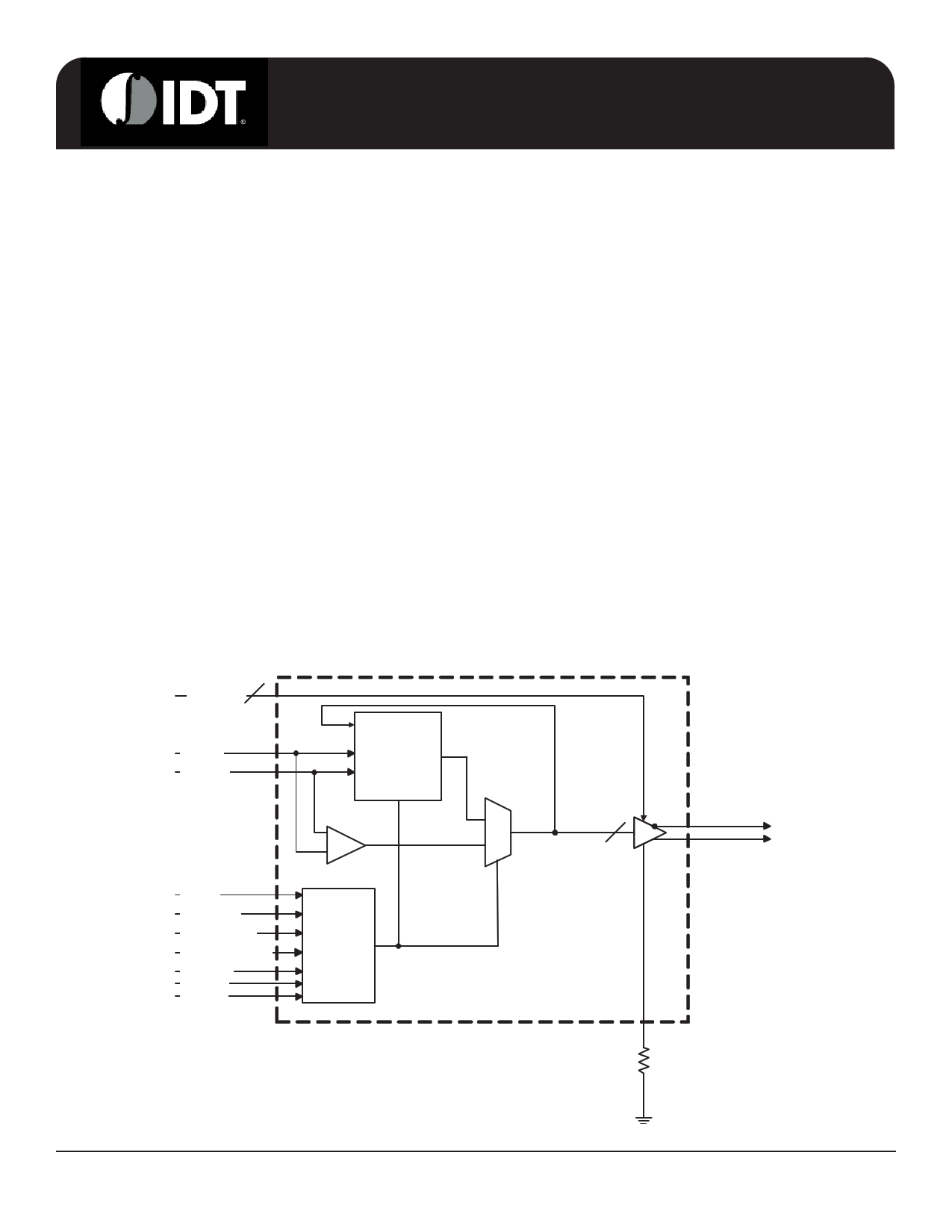
Functional Block Diagram
12
OE_(11:0)#
SRC_IN
SRC_IN#
SPREAD
COMPATIBLE
PLL
FS(2:0)
HIGH_BW#
BYPASS#/PLL
VTTPWRGD#/PD
ADR_SEL
SMBDAT
SMBCLK
CONTROL
LOGIC
M
U
X
12
DIF(11:0))
IREF
IDT® Twelve Output Differential Buffer for PCIe Gen1/Gen2, QPI, and FBDIMM
1
1414F—06/30/10
1 page 
9DB1200C
Twelve Output Differential Buffer for PCIe Gen1/Gen2, QPI, and FBDIMM
Absolute Max
Symbol
VDDA
VDD
VIL
VIH
Ts
Tambient
Tcase
ESD prot
Parameter
3.3V Core Supply Voltage
3.3V Logic Supply Voltage
Input Low Voltage
Input High Voltage
Storage Temperature
Ambient Operating Temp
Case Temperature
Input ESD protection
human body model
Min
GND-0.5
-65
0
2000
Max
4.6
4.6
VDD+0.5V
150
70
115
Units
V
V
V
V
°C
°C
°C
V
Electrical Characteristics - Input/Supply/Common Output Parameters
TA = 0 - 70°C; Supply Voltage VDD = 3.3 V +/-5%
PARAMETER
SYMBOL
CONDITIONS
MIN TYP
Input High Voltage
Input Low Voltage
Input High Current
Input Low Current
VIH 3.3 V +/-5%
2
VIL
3.3 V +/-5%
GND - 0.3
IIH
VIN = VDD
-5
IIL1
VIN = 0 V; Inputs with no pull-up
resistors
-5
IIL2 VIN = 0 V; Inputs with pull-up resistors -200
MAX UNITS NOTES
VDD + 0.3
0.8
5
V
V
uA
1
1
1
uA 1
uA 1
Operating Supply Current IDD3.3OP
Full Active, CL = Full load;
Powerdown Current
IDD3.3PD
all differential pairs tri-stated
Input Frequency
FiPLL
FiBYPASS
PLL Mode
Bypass Mode
Pin Inductance
Lpin
Capacitance
PLL Jitter Peaking
CIN
COUT
jPEAK
Logic Inputs
Output pin capacitance
Peaking when HIGH_BW#=0
Peaking when HIGH_BW#=1
PLL Bandwidth
BW PLL Bandwidth when HIGH_BW#=0
PLL Bandwidth when HIGH_BW#=1
Clk Stabilization
TSTAB
From VDD Power-Up and after input
clock stabilization or de-assertion of
PD# to 1st clock
Modulation Frequency
OE# Latency
fMOD
tLATOE#
Triangular Modulation
DIF start after OE# assertion
DIF stop after OE# deassertion
Tdrive_PD
tDRVPD
DIF output enable after
PD de-assertion
Tfall
tF
Fall time of OE#
Trise
tR
Rise time of OE#
1Guaranteed by design and characterization, not 100% tested in production.
2See timing diagrams for timing requirements.
3Time from deassertion until outputs are >200 mV
IDT® Twelve Output Differential Buffer for PCIe Gen1/Gen2, QPI, and FBDIMM
100
33
1.5
2
0.7
30
4
375 mA
1
24 mA 1
400 MHz 1
400 MHz 1
7 nH 1
5 pF 1
6 pF 1
1.5 2 dB 1
1.5 2 dB 1
3 4 MHz 1
1 1.4 MHz 1
1.8 ms 1,2
33 kHz 1
12 cycles 1,3
300 us 1,3
5 ns 1
5 ns 1
1414F—06/30/10
5
5 Page 
9DB1200C
Twelve Output Differential Buffer for PCIe Gen1/Gen2, QPI, and FBDIMM
SMBus Table: Frequency Select Register
Byte 0 Pin #
Name
Control Function
Bit 7
-
HIGH_BW#
High or Low BW
Bit 6
-
BYPASS#/PLL Bypass (non-PLL Mode) or PLL Mode
Bit 5
-
Reserved
Reserved
Bit 4
-
Reserved
Reserved
Bit 3
-
Reserved
Reserved
Bit 2
-
FS2
Frequency Select 2
Bit 1
-
FS1
Frequency Select 1
Bit 0
-
FS0
Frequency Select 0
Type
RW
RW
RW
RW
RW
RW
RW
RW
01
High BW Low BW
Bypass
PLL
Reserved
Reserved
Reserved
See FS Table
PWD
Latch
Latch
X
X
X
Latch
Latch
Latch
SMBus Table: Output Control Register
Byte 1 Pin #
Name
Bit 7 43,42
DIF_7
Bit 6 38,37
DIF_6
Bit 5 27,28
DIF_5
Bit 4 22,23
DIF_4
Bit 3 19,20
DIF_3
Bit 2 14,15
DIF_2
Bit 1 11,12
DIF_1
Bit 0
6,7
DIF_0
Control Function
Output Control (Disable = Hi-Z)
Output Control (Disable = Hi-Z)
Output Control (Disable = Hi-Z)
Output Control (Disable = Hi-Z)
Output Control (Disable = Hi-Z)
Output Control (Disable = Hi-Z)
Output Control (Disable = Hi-Z)
Output Control (Disable = Hi-Z)
Type
RW
RW
RW
RW
RW
RW
RW
RW
0
Disable
Disable
Disable
Disable
Disable
Disable
Disable
Disable
1
Enable
Enable
Enable
Enable
Enable
Enable
Enable
Enable
PWD
1
1
1
1
1
1
1
1
SMBus Table: Output Control Register
Byte 2 Pin #
Name
Bit 7
-
Reserved
Bit 6
-
Reserved
Bit 5
-
Reserved
Bit 4
-
Reserved
Bit 3 58,59
DIF_11
Bit 2 53,54
DIF_10
Bit 1 50,51
DIF_9
Bit 0 45,46
DIF_8
Control Function
Reserved
Reserved
Reserved
Reserved
Output Control (Disable = Hi-Z)
Output Control (Disable = Hi-Z)
Output Control (Disable = Hi-Z)
Output Control (Disable = Hi-Z)
Type
RW
RW
RW
RW
RW
RW
RW
RW
01
Reserved
Reserved
Reserved
Reserved
Disable Enable
Disable Enable
Disable Enable
Disable Enable
PWD
0
0
0
0
1
1
1
1
SMBus Table: Output Enable Readback
Byte 3 Pin #
Name
Bit 7 43,42
OE7#
Bit 6 38,37
OE6#
Bit 5 27,28
OE5#
Bit 4 22,23
OE4#
Bit 3 19,20
OE3#
Bit 2 14,15
OE2#
Bit 1 11,12
OE1#
Bit 0
6,7
OE0#
Control Function
OE# Pin Readback
OE# Pin Readback
OE# Pin Readback
OE# Pin Readback
OE# Pin Readback
OE# Pin Readback
OE# Pin Readback
OE# Pin Readback
Type
R
R
R
R
R
R
R
R
0
Enabled
Enabled
Enabled
Enabled
Enabled
Enabled
Enabled
Enabled
1
Disabled
Disabled
Disabled
Disabled
Disabled
Disabled
Disabled
Disabled
PWD
X
X
X
X
X
X
X
X
IDT® Twelve Output Differential Buffer for PCIe Gen1/Gen2, QPI, and FBDIMM
11
1414F—06/30/10
11 Page | ||
| Páginas | Total 14 Páginas | |
| PDF Descargar | [ Datasheet 9DB1200C.PDF ] | |
Hoja de datos destacado
| Número de pieza | Descripción | Fabricantes |
| 9DB1200C | Twelve Output Differential Buffer | IDT |
| Número de pieza | Descripción | Fabricantes |
| SLA6805M | High Voltage 3 phase Motor Driver IC. |
Sanken |
| SDC1742 | 12- and 14-Bit Hybrid Synchro / Resolver-to-Digital Converters. |
Analog Devices |
|
DataSheet.es es una pagina web que funciona como un repositorio de manuales o hoja de datos de muchos de los productos más populares, |
| DataSheet.es | 2020 | Privacy Policy | Contacto | Buscar |