|
|
|
PDF MC54HC595A Data sheet ( Hoja de datos )
| Número de pieza | MC54HC595A | |
| Descripción | 8-Bit Serial-Input/Serial or Parallel-Output Shift Register | |
| Fabricantes | Motorola Semiconductors | |
| Logotipo | ||
Hay una vista previa y un enlace de descarga de MC54HC595A (archivo pdf) en la parte inferior de esta página. Total 10 Páginas | ||
|
No Preview Available !
MOTOROLA
SEMICONDUCTOR TECHNICAL DATA
8-Bit Serial-Input/Serial or
Parallel-Output Shift Register
with Latched 3-State Outputs
High–Performance Silicon–Gate CMOS
The MC54/74HC595A is identical in pinout to the LS595. The device
inputs are compatible with standard CMOS outputs; with pullup resistors,
they are compatible with LSTTL outputs.
The HC595A consists of an 8–bit shift register and an 8–bit D–type latch
with three–state parallel outputs. The shift register accepts serial data and
provides a serial output. The shift register also provides parallel data to the
8–bit latch. The shift register and latch have independent clock inputs. This
device also has an asynchronous reset for the shift register.
The HC595A directly interfaces with the Motorola SPI serial data port on
CMOS MPUs and MCUs.
• Output Drive Capability: 15 LSTTL Loads
• Outputs Directly Interface to CMOS, NMOS, and TTL
• Operating Voltage Range: 2.0 to 6.0 V
• Low Input Current: 1.0 µA
• High Noise Immunity Characteristic of CMOS Devices
• In Compliance with the Requirements Defined by JEDEC Standard
No. 7A
• Chip Complexity: 328 FETs or 82 Equivalent Gates
• Improvements over HC595
— Improved Propagation Delays
— 50% Lower Quiescent Power
— Improved Input Noise and Latchup Immunity
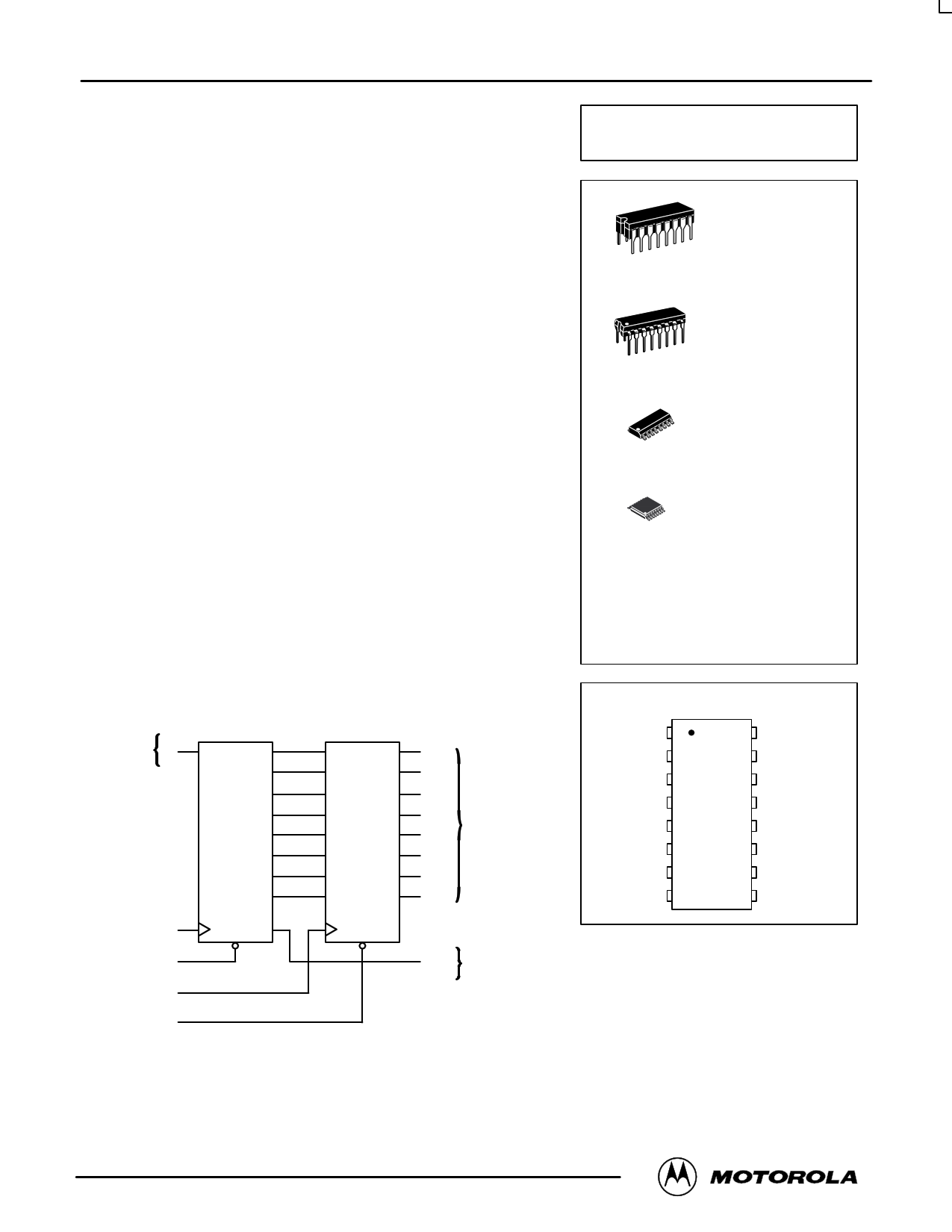
SERIAL
DATA
INPUT
A 14
LOGIC DIAGRAM
SHIFT
REGISTER
LATCH
SHIFT 11
CLOCK
RESET 10
LATCH 12
CLOCK
OUTPUT 13
ENABLE
VCC = PIN 16
GND = PIN 8
15 QA
1 QB
2 QC
3 QD
4 QE
5 QF
6 QG
7 QH
PARALLEL
DATA
OUTPUTS
9 SQH
SERIAL
DATA
OUTPUT
MC54/74HC595A
16
1
J SUFFIX
CERAMIC PACKAGE
CASE 620–10
16
1
N SUFFIX
PLASTIC PACKAGE
CASE 648–08
16
1
D SUFFIX
SOIC PACKAGE
CASE 751B–05
16
1
DT SUFFIX
TSSOP PACKAGE
CASE 948F–01
ORDERING INFORMATION
MC54HCXXXAJ
MC74HCXXXAN
MC74HCXXXAD
MC74HCXXXADT
Ceramic
Plastic
SOIC
TSSOP
PIN ASSIGNMENT
QB 1
QC 2
QD 3
QE 4
QF 5
QG 6
QH 7
GND 8
16 VCC
15 QA
14 A
13 OUTPUT ENABLE
12 LATCH CLOCK
11 SHIFT CLOCK
10 RESET
9 SQH
3/97
© Motorola, Inc. 1997
1
REV 7
1 page 
MC54/74HC595A
FUNCTION TABLE
Operation
Reset shift register
Reset
L
Serial
Input
A
X
Inputs
Shift
Clock
X
Latch
Clock
L, H, ↓
Output
Enable
L
Shift
Register
Contents
L
Resulting Function
Latch
Register
Contents
Serial
Output
SQH
UL
Parallel
Outputs
QA – QH
U
Shift data into shift
register
Shift register remains
unchanged
HD
↑ L, H, ↓ L
D → SRA;
U
SRG → SRH
U
SRN → SRN+1
H X L, H, ↓ L, H, ↓ L
U
U UU
Transfer shift register
contents to latch register
H
X L, H, ↓ ↑
L
U
SRN → LRN
U
SRN
Latch register remains
unchanged
XX
X L, H, ↓ L
*
U *U
Enable parallel outputs X X
X
X
L
*
** * Enabled
Force outputs into high X X
impedance state
X
XH
*
** * Z
SR = shift register contents
LR = latch register contents
D = data (L, H) logic level
U = remains unchanged
↑ = Low–to–High
↓ = High–to–Low
* = depends on Reset and Shift Clock inputs
** = depends on Latch Clock input
PIN DESCRIPTIONS
INPUTS
A (Pin 14)
Serial Data Input. The data on this pin is shifted into the
8–bit serial shift register.
CONTROL INPUTS
Shift Clock (Pin 11)
Shift Register Clock Input. A low– to–high transition on this
input causes the data at the Serial Input pin to be shifted into
the 8–bit shift register.
Reset (Pin 10)
Active–low, Asynchronous, Shift Register Reset Input. A
low on this pin resets the shift register portion of this device
only. The 8–bit latch is not affected.
Latch Clock (Pin 12)
Storage Latch Clock Input. A low–to–high transition on this
input latches the shift register data.
Output Enable (Pin 13)
Active–low Output Enable. A low on this input allows the
data from the latches to be presented at the outputs. A high
on this input forces the outputs (QA–QH) into the high–
impedance state. The serial output is not affected by this
control unit.
OUTPUTS
QA – QH (Pins 15, 1, 2, 3, 4, 5, 6, 7)
Noninverted, 3–state, latch outputs.
SQH (Pin 9)
Noninverted, Serial Data Output. This is the output of the
eighth stage of the 8–bit shift register. This output does not
have three–state capability.
High–Speed CMOS Logic Data
DL129 — Rev 6
5
MOTOROLA
5 Page | ||
| Páginas | Total 10 Páginas | |
| PDF Descargar | [ Datasheet MC54HC595A.PDF ] | |
Hoja de datos destacado
| Número de pieza | Descripción | Fabricantes |
| MC54HC595A | 8-Bit Serial-Input/Serial or Parallel-Output Shift Register | Motorola Semiconductors |
| Número de pieza | Descripción | Fabricantes |
| SLA6805M | High Voltage 3 phase Motor Driver IC. |
Sanken |
| SDC1742 | 12- and 14-Bit Hybrid Synchro / Resolver-to-Digital Converters. |
Analog Devices |
|
DataSheet.es es una pagina web que funciona como un repositorio de manuales o hoja de datos de muchos de los productos más populares, |
| DataSheet.es | 2020 | Privacy Policy | Contacto | Buscar |