|
|
|
PDF BD18340FV-M Data sheet ( Hoja de datos )
| Número de pieza | BD18340FV-M | |
| Descripción | Constant Current Controller | |
| Fabricantes | ROHM Semiconductor | |
| Logotipo | ||
Hay una vista previa y un enlace de descarga de BD18340FV-M (archivo pdf) en la parte inferior de esta página. Total 30 Páginas | ||
|
No Preview Available !
Datasheet
Constant Current LED Drivers for Automotive
Constant Current Controller
for Automotive LED Lamps
BD18340FV-M BD18341FV-M
General Description
BD18340FV-M/BD18341FV-M are 70V-withstanding
Constant Current Controller for Automotive LED Lamps.
It is able to drive at maximum 10 rows of PNP transistors.
It can also contribute to reduction in the consumption
power of the set as it has the integrated standby function.,
The IC also incorporates a highly reliable, in-built
de-rating function, LED Open Detection, Short Circuit
Protection and Over Voltage Mute function and LED
failure input/output function.
Features
AEC-Q100 Qualified(Note1)
LED Constant-Current Controller
PWM Dimming Function
LED Current De-rating Function
LED Open Detection
Short Circuit Protection(SCP)
Over Voltage Mute Function(OVM)
Disable LED Open Detection Function at
Reduced-Voltage
Abnormal Output Detection and Output Functions
(Note1: Grade1)
Applications
Automotive LED Exterior Lamp
(Rear Lamp, Turn Lamp, DRL/Position Lamp,
Fog Lamp etc.)
Automotive LED Interior Lamp
(Air Conditioner Lamp, Interior Lamp,
Cluster Light etc.)
Key Specifications
Input Voltage Range:
4.5V to 19V
FB Terminal Voltage Accuracy:
650mV ±3%
@Ta = 25°C to 125°C
Stand-by Current:
0µA(Typ)
LED Current De-rating Accuracy:
BD18340FV-M : ± 5% @VDCDIM=0.5 to 0.75V
BD18341FV-M : ±12% @VDCDIM=0.5 to 0.75V
Operating Temparature Range: -40°C to +125°C
Package
SSOP-B16
W(Typ) x D(Typ) x H(Max)
5.00mm x 6.40mm x 1.35mm
SSOP-B16
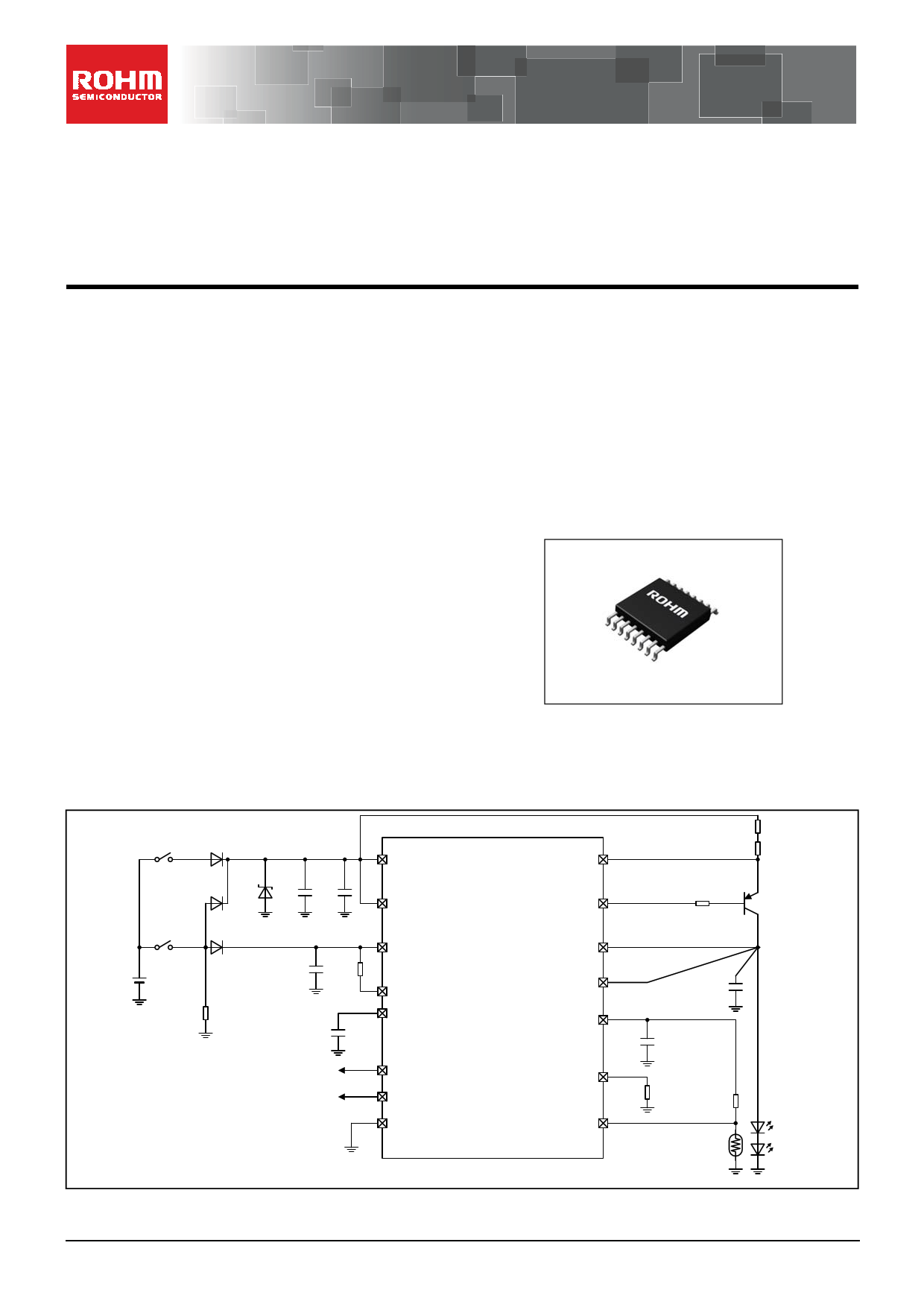
Typical Application Circuit
PWM_in
D1
ZD1
D2
CVIN1 CVIN2
DC_in
D3
CCRT
RCRT
RDCIN
CD
VIN FB
EN BASE
CRT
OP
DISC BD18340FV-M SCP
D BD18341FV-M VREG
CVREG
PWMOUT
PBUS
OPM
ROPM
GND
DCDIM
RFB1
RFB2
RLIM
CLED
RDCDIM
NTC
〇Product structure : Silicon monolithic integrated circuit
www.rohm.co.jp
©2016 ROHM Co., Ltd. All rights reserved.
TSZ22111・14・001
〇This product has no designed protection against radioactive rays
1/35
TSZ02201-0T1T0C700180-1-2
2016.04.21 Rev.002
1 page 
BD18340FV-M BD18341FV-M
Datasheet
Electrical Characteristics1
(Unless otherwise specified Ta = -40 to +125°C, VIN = 13V, CVREG = 1.0µF, Transistor PNP = 2SAR573D)
Parameter
Symbol
Min
Limit
Typ
Max Unit
Conditions
[ Circuit Current IVIN ]
Circuit Current
at Stand-by Mode
Circuit Current
at Normal Mode
Circuit Current
at LED Open Detection
Circuit Current
at PBUS=Low
IVIN1
IVIN2
IVIN3
IVIN4
-
-
-
-
0
10
μA
VEN = 0V
VFB=VIN
2.0
5.0
mA
VEN = VIN, VFB=VIN-1.0V
Base current subtracted
2.0
5.0
mA
VEN = VIN, VFB=VIN-1.0V
at LED Open Detection
2.0
5.0
mA
VEN = VIN, VFB=VIN-1.0V
VPBUS = 0V
[ VREG Voltage ]
VREG Terminal Voltage
VREG Terminal
Current Capability
[ DRV ]
FB Terminal Voltage
FB Terminal
Input Current
BASE Terminal Sink
Current Capability
VREG
IVREG
4.85
4.75
-1.0
VFBREG
IFB
IBASE
630
617
7.5
10
5.00
5.00
-
650
650
15
-
5.15
5.25
-
670
683
30
-
V
IVREG = -100μA
Ta = 25 to 125°C
V
IVREG = -100μA
Ta = -40 to 125°C
mA
VFBREG = VIN - VFB
mV RFB1 = RFB2 = 1.8Ω,
Ta = 25 to 125°C
VFBREG = VIN - VFB
mV RFB1 = RFB2 = 1.8Ω,
Ta = -40 to 125°C
μA VFB = VIN
mA
VFB = VIN, VBASE = VIN - 1.5V
Ta = 25°C
BASE Terminal
Pull-up Resistor
RBASE
0.5
1.0
1.5
kΩ
VCRT = 0V
VFB = VIN, VBASE = VIN - 1.0V
[ LED Current De-rating Function (DC Dimming Function) ]
DC Dimming Gain
DDG 688 725
BD18340FV-M
FB Terminal Voltage
VDCDIM = 0.75V
FB Terminal Voltage
VDCDIM = 0.50V
FB Terminal Voltage
VDCDIM = 0.35V
VFB_DC1
VFB_DC2
VFB_DC3
443
270
161
466
284
175
762
mV / ⊿VFBREG / ⊿VDCDIM
V VDCDIM:0.75V -> 0.35V
489 mV
298 mV
189 mV
BD18341FV-M
FB Terminal Voltage
VDCDIM = 0.75V
FB Terminal Voltage
VDCDIM = 0.50V
FB Terminal Voltage
VDCDIM = 0.35V
VFB_DC1
413
466
522 mV
VFB_DC2
250
284
318 mV
VFB_DC3
155
175
196 mV
[ Over Voltage Mute Function(OVM) ]
Over Voltage Mute
Start Voltage
Over Voltage Mute
Gain
VOVMS
VOVMG
20.0
-
22.0
-25
24.0
-
∆VFB = 10.0mV
V ∆VFB = VFB(@VIN = 13V) –
VFB(@VIN = VOVM)
mV /
V
∆VFB / ∆VIN
www.rohm.co.jp
©2016 ROHM Co., Ltd. All rights reserved.
TSZ22111・14・001
5/35
TSZ02201-0T1T0C700180-1-2
2016.04.21 Rev.002
5 Page 
BD18340FV-M BD18341FV-M
Datasheet
Features Description
(Unless otherwise specified, Ta=25°C, VIN=13V, Transistor PNP = 2SAR573D, and numbers are “Typical” values.)
1. LED Current Setting
LED current ILED can be defined by setting resistances RFB1 and RFB2.
where:
VFBREG is the FB Terminal Voltage 650mV (Typ)
・How to connect LED current setting resistors
LED current setting resistors must always be connected at least in pair arranged in series as below.
If only one current setting resistor is used, then in case of a possible resistor short, the external PNP Tr. and LED
may be broken due to large current flow.
PNP Tr. rating current, LED rating current, RFB1 and RFB2 must have the following relations:
__
,
where:
ILED_Max is the LED Rating Current
IPNP_Max is the PNP Tr. Rating Current
VFBREG is the FB Terminal Voltage 650mV(Typ)
Min RFB1,RFB2 is the Lowest value of RFB1 and RFB2
VIN
+B EN
VREG
C VREG
VREG
GND
VREF
FB
BASE
R FB1
R FB2
VCE(SAT)
ILED
Figure 13. LED Current Setting
・Constant current control dynamic range
Constant current control dynamic range of LED current ILED can be calculated as follows.
_∙
_
where:
VIN is the VIN Terminal Voltage
Vf_LED is the LED Vf
N is the Number of Rows of LED
VCE sat is the External PNP Tr. Collector-Emitter Saturation Voltage
VFBREG is the FB Terminal Voltage 650mV(Typ)
2. Reference-Voltage (VREG)
VIN terminal generates 5.0V (Typ). This voltage is used as power source for the internal circuit, and also used to fix the
voltage of terminals outside LSI to HIGH side. VREG terminal must be connected with CVREG = 1.0μF to 4.7μF to ensure
capacity for the phase compensation. If CVREG is not connected, the circuit behavior would become extraordinarily unstable,
for example with the oscillation of the reference-voltage.
VREG terminal voltage must not be used as power source for other devices than this LSI.
VREG circuit has a built-in UVLO function. The IC is activated when the VREG terminal voltage rises to 4.0V (Typ) or higher,
and shut down when the VREG terminal voltage drops to 3.75V(Typ) or lower.
www.rohm.co.jp
©2016 ROHM Co., Ltd. All rights reserved.
TSZ22111・14・001
11/35
TSZ02201-0T1T0C700180-1-2
2016.04.21 Rev.002
11 Page | ||
| Páginas | Total 30 Páginas | |
| PDF Descargar | [ Datasheet BD18340FV-M.PDF ] | |
Hoja de datos destacado
| Número de pieza | Descripción | Fabricantes |
| BD18340FV-M | Constant Current Controller | ROHM Semiconductor |
| Número de pieza | Descripción | Fabricantes |
| SLA6805M | High Voltage 3 phase Motor Driver IC. |
Sanken |
| SDC1742 | 12- and 14-Bit Hybrid Synchro / Resolver-to-Digital Converters. |
Analog Devices |
|
DataSheet.es es una pagina web que funciona como un repositorio de manuales o hoja de datos de muchos de los productos más populares, |
| DataSheet.es | 2020 | Privacy Policy | Contacto | Buscar |