|
|
|
PDF STD1807 Data sheet ( Hoja de datos )
| Número de pieza | STD1807 | |
| Descripción | Synchronous Step Down DC/DC Converter | |
| Fabricantes | Semtron | |
| Logotipo | ||
Hay una vista previa y un enlace de descarga de STD1807 (archivo pdf) en la parte inferior de esta página. Total 8 Páginas | ||
|
No Preview Available !
STD1807
■DESCRIPTION
1.5MHz, 1.5A, Synchronous Step Down DC/DC Converter
■FEATURE
The STD1807 is a high-efficiency, DC-to-DC
step-down switching regulators, capable of
delivering up to 1.5A of output current. The device
operates from an input voltage range of 2.5V to
6.0V and provides an output voltage from 0.6V to
VIN, making the STD1807 ideal for low voltage
power conversions. Running at a fixed frequency of
1.5MHz allows the use of small external
components, such as ceramic input and output
caps, as well as small inductors, while still providing
low output ripples. This low noise output along with
its excellent efficiency achieved by the internal
synchronous rectifier, making STD1807 an ideal
green replacement for large power consuming
linear regulators. Internal soft-start control circuitry
reduces inrush current. Short-circuit and thermal-
overload protection improves design reliability.
STD1807S5-TRG ROHS Compliant This is Halogen
Free
Duty Cycle 0~100%
1.5A Output Current
High Efficiency Up To 96%
2.5V to 6.0V Input Voltage Range
Fixed 1.5MHz Frequency
Logic Control Shutdown IQ<1μA
Thermal Shutdown
Output Adjustable from 0.6V to Input Voltage
■APPLICATIONS
Digital Framer
PDA and Pocket PC
Cellular Phone and Smart Phone
Wireless Devices
Battery Powered Widgets
Portable Media Players
Electronic Scales
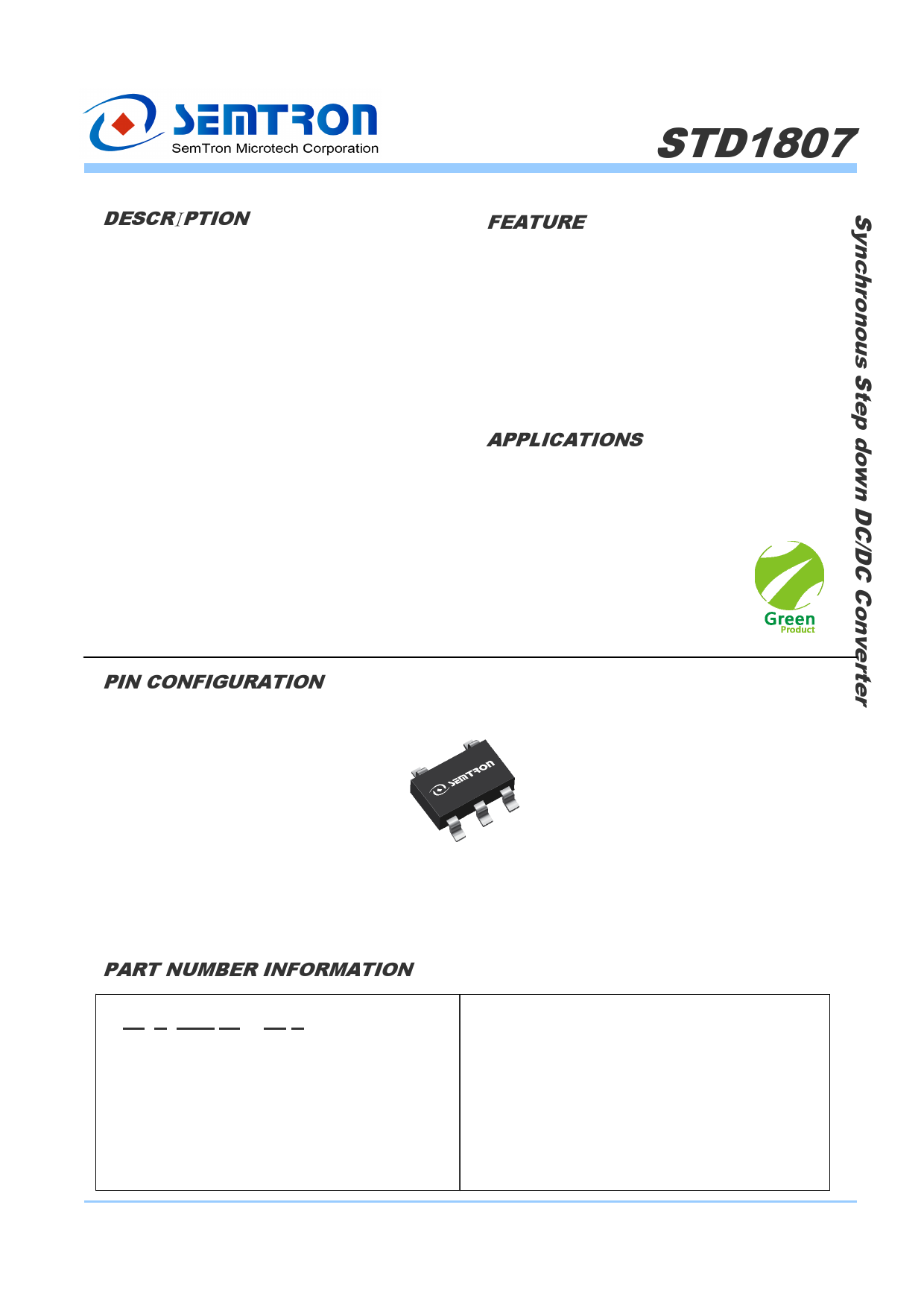
■PIN CONFIGURATION
VIN
FB
SW
GND
EN
SOT-23 -5L
Top View
■PART NUMBER INFORMATION
ST D 1807 S5 – TR G
ab c d ef
a : Company name.
b : Product type.
c : Product Serial number.
d : Package Code
e : Handling Code
f : Lead Plating Code
G : Lead-free product
This product is Halogen Free
STD1807 Rev.1.4
Copyright © Semtron Microtech Corp.
1
www.semtron-micro.com
1 page 
■DESIGN PROCEDURE
◆Setting Output Voltage
Output voltages are set by external resistors. The
FB hreshold is 0.8V.
RTOP = RBOTTOM[(VOUT / 0.6) - 1]
◆Input Capacitor Selection
The input capacitor in a DC-to-DC converter
reduces current peaks drawn from the battery or
other input power source and reduces switching
noise in the controller. The impedance of the input
capacitor at the switching frequency should be less
than that of the input source so high-frequency
switching currents do not pass through the input
source. The output capacitor keeps output ripple
small and ensures control-loop stability. The output
capacitor must also have low impedance at the
switching frequency. Ceramic, polymer, and
tantalum capacitors are suitable, with ceramic
exhibiting the lowest ESR and high-frequency
impedance. Output ripple with a ceramic output
capacitor is approximately as follows:
STD1807
VRIPPLE = IL(PEAK)[1 / (2π x fOSC x COUT)]
If the capacitor has significant ESR, the output
ripple component due to capacitor ESR is as follows:
VRIPPLE(ESR) = IL(PEAK) x ESR
◆Output Capacitor and Inductor Selection
Follow the below table for Inductor and Output
cap selection:
VOUT
COUT
L
1.2V
33μF
1.5μH
1.5V
33μF
1.5μH
1.8V
10~22μF
2.2μH
2.5V
10~22μF
3.3μH
3.3V
10μF
4.7μH
If much smaller values are used, inductor current
rises, and a larger output capacitance may be
required to suppress output ripple. Larger values
than LIDEAL can be used to obtain higher output
current, but typically with larger inductor size.
■APPLICAITION INFORMATION
Layout is critical to achieve clean and stable
operation. The switching power stage requires
particular attention. Follow these guidelines for good
PC board layout:
1) Place decoupling capacitors as close to the IC
as possible. Keep power ground plane (connected
to PGND) and signal ground plane (connected to
GND) separate.
2) Connect input and output capacitors to the
power ground plane; connect all other capacitors to
the signal ground plane.
3) Keep the high-current paths as short and wide
as possible. Keep the path of switching current (C1
to IN and C1 to GND) short. Avoid vias in the
switching paths.
4) If possible, connect VIN, SW, and GND
separately to a large copper area to help cool the IC
to further improve efficiency and long-term reliability.
5) Ensure all feedback connections are short and
direct. Place the feedback resistors as close to the
IC as possible.
6) Route high-speed switching nodes away from
sensitive analog areas
STD1807 Rev.1.4
Copyright © Semtron Microtech Corp.
www.semtron-micro.com
5 Page | ||
| Páginas | Total 8 Páginas | |
| PDF Descargar | [ Datasheet STD1807.PDF ] | |
Hoja de datos destacado
| Número de pieza | Descripción | Fabricantes |
| STD1802 | Low voltage fast-switching NPN power transistor | STMicroelectronics |
| STD1802T4 | Low voltage fast-switching NPN power transistor | STMicroelectronics |
| STD1802T4-A | Low voltage fast-switching NPN power transistor | STMicroelectronics |
| STD1805 | LOW VOLTAGE FAST-SWITCHING NPN POWER TRANSISTOR | STMicroelectronics |
| Número de pieza | Descripción | Fabricantes |
| SLA6805M | High Voltage 3 phase Motor Driver IC. |
Sanken |
| SDC1742 | 12- and 14-Bit Hybrid Synchro / Resolver-to-Digital Converters. |
Analog Devices |
|
DataSheet.es es una pagina web que funciona como un repositorio de manuales o hoja de datos de muchos de los productos más populares, |
| DataSheet.es | 2020 | Privacy Policy | Contacto | Buscar |